
AX1000-BGG729I
| Part Description |
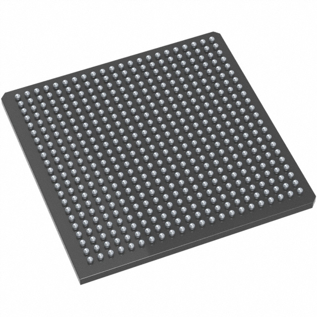
Axcelerator Field Programmable Gate Array (FPGA) IC 516 165888 729-BBGA |
|---|---|
| Quantity | 892 Available (as of June 15, 2026) |

| Product Category | Field Programmable Gate Array (FPGA) |
|---|---|
| Manufacturer | Microchip Technology |
| Manufacturing Status | Active |
| Manufacturer Standard Lead Time | 52 Weeks |
| Datasheet |
Specifications & Environmental
| Device Package | 729-PBGA (35x35) | Grade | Industrial | Operating Temperature | -40°C – 85°C | ||
|---|---|---|---|---|---|---|---|
| Package / Case | 729-BBGA | Number of I/O | 516 | Voltage | 1.425 V - 1.575 V | ||
| Mounting Method | Surface Mount | RoHS Compliance | ROHS3 Compliant | REACH Compliance | REACH Unaffected | ||
| Moisture Sensitivity Level | 3 (168 Hours) | Number of LABs/CLBs | 18144 | Number of Logic Elements/Cells | 18144 | ||
| Number of Gates | 1000000 | ECCN | 3A001A7A | HTS Code | 8542.39.0001 | ||
| Qualification | N/A | Total RAM Bits | 165888 |
Overview of AX1000-BGG729I – Axcelerator Field Programmable Gate Array IC, 516 I/Os, 165,888-bit Embedded RAM, 729-BBGA
The AX1000-BGG729I is an Axcelerator antifuse FPGA implementing Microchip's AX architecture as a single-chip, nonvolatile programmable logic solution. It delivers high-density logic (1,000,000 equivalent system gates) with 18,144 logic elements and embedded SRAM/FIFO resources suitable for industrial designs.
Designed for system-level integration, the device offers segmentable clocks, on-chip PLLs, high-speed I/Os and deterministic timing for applications that require secure, high-performance programmable logic in a surface-mount 729-BBGA package.
Key Features
- Core Capacity — 1,000,000 equivalent system gates with 18,144 logic elements and up to 12,096 flip-flops, providing substantial programmable logic density for complex designs.
- Embedded Memory — 165,888 bits of on-chip SRAM/FIFO (approximately 0.166 Mbits) with variable-aspect 4,608-bit RAM blocks and embedded FIFO control logic for buffering and packet handling.
- I/O Flexibility — 516 user I/Os with bank-selectable I/O architecture (8 banks per chip) and mixed-voltage operation (1.5V, 1.8V, 2.5V, 3.3V); supports single-ended and differential standards including LVTTL, LVCMOS, LVDS and LVPECL.
- High-Speed Performance — Datasheet-specified system performance of 350+ MHz and internal performance above 500+ MHz, plus LVDS-capable I/Os up to 700 Mb/s for high-throughput interfaces.
- Clocking and PLLs — Segmentable clock resources and embedded PLLs with an input range of 14–200 MHz and frequency synthesis capability up to 1 GHz to support complex timing architectures.
- Nonvolatile Antifuse Technology & Security — Single-chip nonvolatile antifuse programming and FuseLock programming technology to protect designs against reverse engineering and unauthorized access.
- Deterministic Timing & Debug — Deterministic, user-controllable timing and in-system diagnostic/debug capability with Microchip Silicon Explorer II to streamline validation and bring-up.
- Package, Power and Temperature — Surface-mount 729-BBGA (supplier package: 729-PBGA, 35 × 35 mm), core supply 1.425 V to 1.575 V (nominal 1.5 V), industrial operating range −40 °C to +85 °C, RoHS compliant.
Typical Applications
- High-performance digital processing — Large logic capacity and high internal/system performance enable processing engines and protocol offloads that require substantial programmable logic resources.
- Secure embedded systems — Single-chip nonvolatile antifuse programming and FuseLock protection are suited to designs where IP protection and reverse-engineering resistance are required.
- High-speed interface bridging — 516 flexible I/Os and LVDS-capable channels support high-throughput serial and parallel interfaces for protocol conversion and board-level bridging.
- Buffered data transport and FIFO handling — Integrated SRAM/FIFO blocks with programmable FIFO control simplify packet buffering, stream alignment and memory-mapped data paths.
Unique Advantages
- Highly integrated single-chip solution: Combines logic, embedded RAM/FIFO, PLLs and high-speed I/Os to reduce external components and simplify system design.
- Deterministic timing and on-chip debug: User-controllable timing and Microchip's Silicon Explorer II support shorten debug cycles and improve time-to-market.
- Flexible I/O standards: Bank-selectable mixed-voltage I/Os and support for multiple single-ended and differential standards enable broad interface compatibility without external translators.
- Nonvolatile security: Antifuse technology and FuseLock programming protect design assets and provide a persistent, tamper-resistant configuration.
- Industrial-grade operation: Specified for −40 °C to +85 °C operation and surface-mount 729-BBGA packaging for reliable deployment in industrial environments.
Why Choose AX1000-BGG729I?
The AX1000-BGG729I positions as a high-density, nonvolatile FPGA with features tailored for secure, deterministic and high-performance embedded systems. Its combination of 1,000,000 equivalent gates, 18,144 logic elements, substantial embedded RAM/FIFO, and flexible high-speed I/Os supports complex designs that require both throughput and configurability.
With antifuse programming technology, on-chip PLLs, and diagnostic/debug support, this device is well suited to designers seeking a robust programmable logic component for industrial applications where long-term stability, IP protection and reliable timing are priorities.
Request a quote or submit a purchasing inquiry today to evaluate AX1000-BGG729I for your design needs.


Date Founded: 1989
Headquarters: Chandler, Arizona, USA
Employees: 22,000+
Revenue: $8.349 Billion
Certifications and Memberships: ISO9001:2015, IATF16949:2016, AS 9100D


