
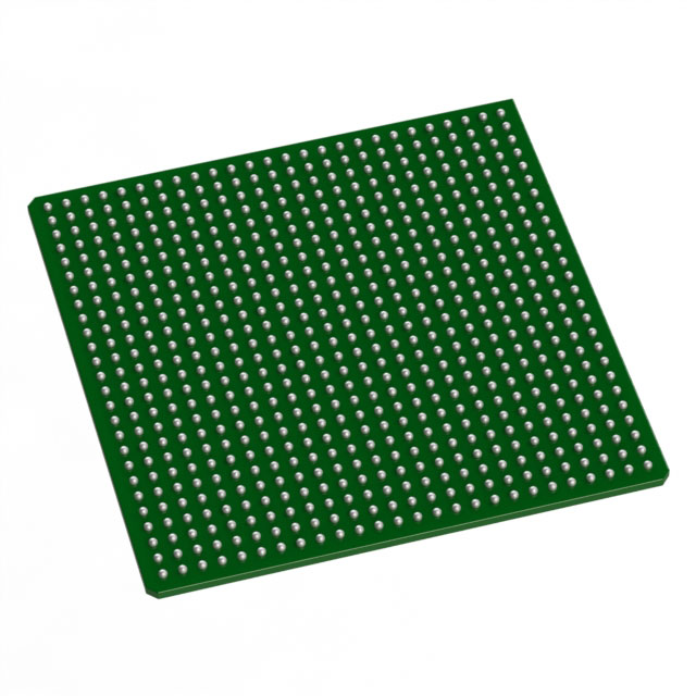
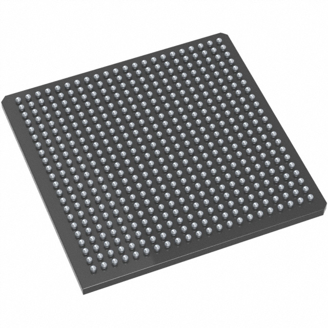
AX1000-CQ352M
| Part Description |
Axcelerator Field Programmable Gate Array (FPGA) IC 198 165888 352-BFCQFP with Tie Bar |
|---|---|
| Quantity | 751 Available (as of June 10, 2026) |

| Product Category | Field Programmable Gate Array (FPGA) |
|---|---|
| Manufacturer | Microchip Technology |
| Manufacturing Status | Active |
| Manufacturer Standard Lead Time | 44 Weeks |
| Datasheet |
Specifications & Environmental
| Device Package | 352-CQFP (75x75) | Grade | Military | Operating Temperature | -55°C – 125°C | ||
|---|---|---|---|---|---|---|---|
| Package / Case | 352-BFCQFP with Tie Bar | Number of I/O | 198 | Voltage | 1.425 V - 1.575 V | ||
| Mounting Method | Surface Mount | RoHS Compliance | RoHS non-compliant | REACH Compliance | REACH Unaffected | ||
| Moisture Sensitivity Level | 3 (168 Hours) | Number of LABs/CLBs | 18144 | Number of Logic Elements/Cells | 18144 | ||
| Number of Gates | 1000000 | ECCN | 3A001A2C | HTS Code | 8542.39.0001 | ||
| Qualification | N/A | Total RAM Bits | 165888 |
Overview of AX1000-CQ352M – Axcelerator Field Programmable Gate Array (FPGA) IC 198 165888 352-BFCQFP with Tie Bar
The AX1000-CQ352M is an Axcelerator antifuse FPGA implementing Microchip's AX architecture as a single-chip, nonvolatile programmable logic device. It delivers deterministic timing, on-chip embedded memory and FIFOs, and architecture-level security for designs that require stable, one-time-programmable logic.
Targeted at applications that demand secure, high-performance programmable logic in harsh environments, the device provides 1,000,000 gates, 18,144 logic elements, 198 user I/Os, and approximately 0.166 Mbits of embedded memory. It is supplied in a 352-BFCQFP with tie bar surface-mount package and is rated for military temperature operation.
Key Features
- Core Architecture Antifuse Axcelerator (AX) architecture offering a single-chip, nonvolatile implementation with 1,000,000 equivalent system gates and 18,144 logic elements for complex logic integration.
- Embedded Memory & FIFOs Approximately 0.166 Mbits of embedded SRAM/FIFO implemented as variable-aspect 4,608-bit RAM blocks; embedded FIFO control logic is supported for high-throughput buffering.
- I/O Flexibility 198 user I/Os with bank-selectable multi-voltage operation (1.5V, 1.8V, 2.5V, 3.3V), support for single-ended and differential standards (including LVDS and LVPECL), registered I/Os, and programmable drive/slew settings.
- Clocking & PLL Segmentable clock resources and an embedded PLL with a 14–200 MHz input range and frequency synthesis capabilities up to 1 GHz for flexible clocking and timing architectures.
- Performance Series-level performance characteristics include 350+ MHz system performance and 500+ MHz internal performance to support timing-critical designs.
- Security & Reliability FuseLock™ programming technology for protection against reverse engineering, single-chip nonvolatile configuration, and military-grade operating temperature range (−55°C to 125°C).
- Package & Power Surface-mount 352-BFCQFP with tie bar (supplier package 352-CQFP, 75×75). Core supply voltage specified at 1.425 V to 1.575 V and RoHS compliant.
Typical Applications
- Military and Aerospace Systems Military-grade temperature range and FuseLock security make the device suitable for secure, ruggedized systems that require nonvolatile programmable logic.
- High-Speed Serial Interfaces LVDS-capable I/Os (700 Mb/s capable per series) and embedded FIFO support enable implementation of high-speed serial links and serial deserialization/serialization functions.
- Network & Communications High internal performance and PLL frequency synthesis support timing-critical packet processing, protocol handling, and custom network functions.
- Instrumentation & Test Equipment Deterministic timing, embedded FIFOs and on-chip diagnostic capabilities support precision data capture, buffering and deterministic control tasks.
Unique Advantages
- Design Security: FuseLock programming protects bitstream IP and helps prevent reverse engineering.
- Nonvolatile, Single-Chip Solution: Antifuse architecture provides persistent configuration without external configuration memory.
- Wide Operating Temperature: Rated −55°C to 125°C for deployment in harsh and mission-critical environments.
- Deterministic Timing & Diagnostics: User-controllable timing and in-system diagnostic/debug capability with Microchip tools for predictable system behavior and observability.
- Flexible I/O Standards: Bank-selectable multi-voltage I/Os and support for differential and single-ended standards simplify interface design across mixed-voltage systems.
- Compact Surface-Mount Packaging: 352-BFCQFP with tie bar enables board-level integration while matching the mechanical and thermal needs of demanding designs.
Why Choose AX1000-CQ352M?
The AX1000-CQ352M is positioned for designs that require secure, high-density programmable logic with deterministic timing and on-chip memory/FIFO resources. Its antifuse, single-chip nonvolatile architecture and FuseLock programming provide hardware-level IP protection while the device’s performance characteristics support timing-sensitive and high-throughput applications.
Part of the Axcelerator family, this device is suitable for customers building military, communications, and instrumentation systems who need a robust, long-term programmable solution with integrated clocking, flexible I/O, and diagnostics.
Request a quote or submit an inquiry to receive pricing and availability information for the AX1000-CQ352M.


Date Founded: 1989
Headquarters: Chandler, Arizona, USA
Employees: 22,000+
Revenue: $8.349 Billion
Certifications and Memberships: ISO9001:2015, IATF16949:2016, AS 9100D


