
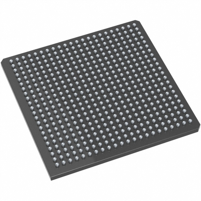
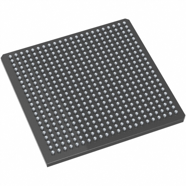
AX1000-FG676
| Part Description |
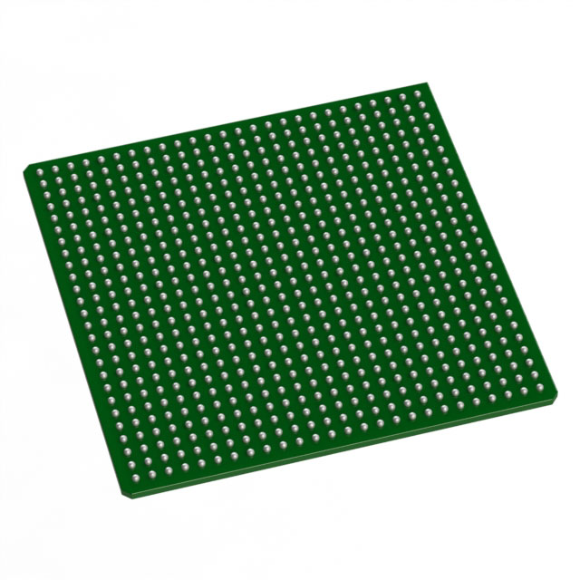
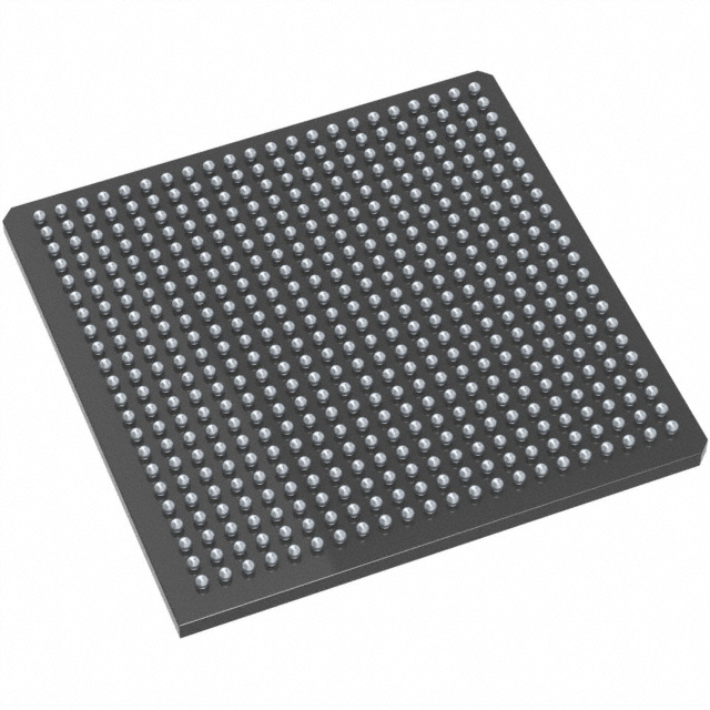
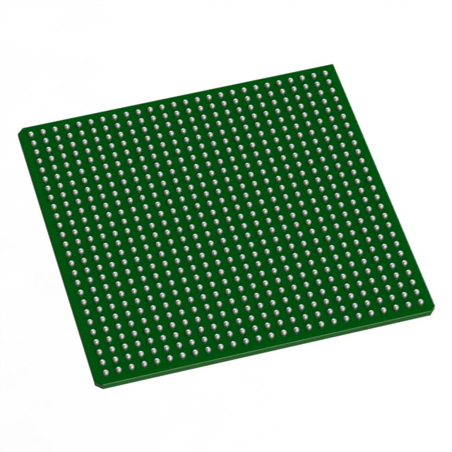
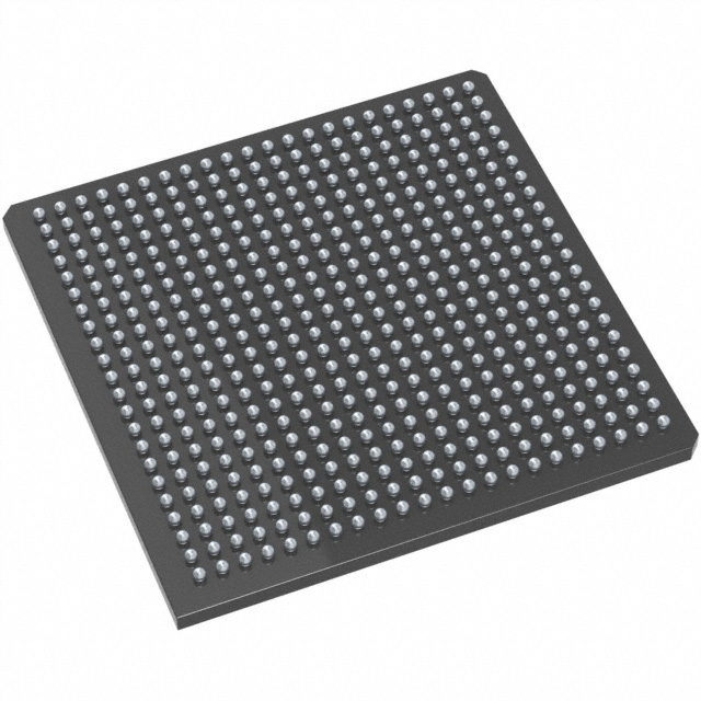
Axcelerator Field Programmable Gate Array (FPGA) IC 418 165888 676-BGA |
|---|---|
| Quantity | 1,861 Available (as of October 7, 2026) |
| Product Category | Field Programmable Gate Array (FPGA) |
|---|---|
| Manufacturer | Microchip Technology |
| Manufacturing Status | Active |
| Manufacturer Standard Lead Time | 12 Weeks |
| Datasheet |
Specifications & Environmental
| Device Package | 676-FBGA (27x27) | Grade | Commercial | Operating Temperature | 0°C – 70°C | ||
|---|---|---|---|---|---|---|---|
| Package / Case | 676-BGA | Number of I/O | 418 | Voltage | 1.425 V - 1.575 V | ||
| Mounting Method | Surface Mount | RoHS Compliance | RoHS non-compliant | REACH Compliance | REACH Unaffected | ||
| Moisture Sensitivity Level | 3 (168 Hours) | Number of LABs/CLBs | 18144 | Number of Logic Elements/Cells | 18144 | ||
| Number of Gates | 1000000 | ECCN | 3A001A7A | HTS Code | 8542.39.0001 | ||
| Qualification | N/A | Total RAM Bits | 165888 |
Overview of AX1000-FG676 – Axcelerator Field Programmable Gate Array (FPGA) IC 418 165888 676-BGA
The AX1000-FG676 is an Axcelerator-series antifuse FPGA based on Microchip’s AX architecture. It combines high gate density with deterministic, nonvolatile antifuse programming to address demanding designs that require high performance and design security.
Designed for commercial applications, the device provides a balance of system performance, embedded memory and flexible I/O in a 676‑ball BGA package, making it suitable for high-speed logic, interface bridging and system integration tasks.
Key Features
- Core capacity and logic elements — Approximately 1,000,000 equivalent system gates with 18,144 logic elements, enabling substantial logic integration on a single device.
- Embedded memory — Approximately 0.166 Mbits of embedded SRAM/FIFO (165,888 total bits) with variable-aspect 4,608-bit RAM blocks and programmable FIFO control logic.
- High-performance timing — Family-level performance indicators include 350+ MHz system performance and 500+ MHz internal performance; deterministic and user-controllable timing supports predictable design behavior.
- Flexible I/O — 418 user I/Os with multi-standard, bank-selectable I/O options (supporting multiple voltage references and registered I/Os); LVDS-capable channels for high-speed serial links.
- Embedded clocking and PLLs — Segmentable clock resources and embedded PLLs with a 14–200 MHz input range and frequency synthesis capability up to 1 GHz for flexible clock management.
- Nonvolatile antifuse technology — Single-chip, nonvolatile programming using antifuse technology and FuseLock™ programming to protect against reverse engineering and improve design security.
- Power and supply — Core supply 1.425 V to 1.575 V with a nominal 1.5 V core voltage; designed for low-power single-chip nonvolatile operation.
- Package & mounting — 676‑BGA (supplier device package: 676‑FBGA, 27 × 27 mm) surface-mount package suitable for high-density board designs.
- Commercial temperature grade — Rated for 0 °C to 70 °C operating temperature and RoHS compliant.
Typical Applications
- High‑speed interface bridging — Supports high-speed serial links and LVDS-capable I/Os, making it suitable for protocol bridging and interface aggregation.
- Data path and packet processing — Large logic capacity and embedded FIFOs enable implementation of packet-handling logic and custom datapaths.
- Prototyping and ASIC replacement — High gate density and deterministic timing allow designers to implement complex systems previously targeted to ASICs while retaining FPGA flexibility.
- Secure, nonvolatile logic — Antifuse nonvolatile programming and FuseLock protect intellectual property in security-sensitive applications.
Unique Advantages
- High integration in a single device: Consolidates up to 1,000,000 equivalent system gates and 18,144 logic elements, reducing BOM count and board complexity.
- Deterministic timing and embedded PLLs: Segmentable clocks and on-chip PLLs provide precise, controllable timing for performance-critical systems.
- Embedded FIFO and RAM flexibility: Configurable RAM block aspect ratios and programmable FIFO control simplify memory interfacing and buffering tasks.
- Nonvolatile, secure programming: Antifuse technology with FuseLock reduces risk of reverse engineering and secures deployed designs.
- Commercial-ready package and compliance: Surface-mount 676‑BGA package and RoHS compliance support modern PCB assembly and environmental requirements.
Why Choose AX1000-FG676?
The AX1000-FG676 positions itself as a high-capacity, nonvolatile FPGA optimized for applications that require substantial logic resources, embedded memory and robust timing control. Its antifuse-based AX architecture delivers deterministic behavior and design security while providing the performance and I/O flexibility needed for demanding system designs.
This device is well suited for engineers and system integrators who need a single-chip solution that balances gate density, embedded memory and high-speed I/O in a commercial-temperature, RoHS-compliant package—helping reduce system complexity and protect intellectual property over the product lifetime.
Request a quote or submit a product inquiry to evaluate the AX1000-FG676 for your next design.





















Date Founded: 1989
Headquarters: Chandler, Arizona, USA
Employees: 22,000+
Revenue: $8.349 Billion
Certifications and Memberships: ISO9001:2015, IATF16949:2016, AS 9100D




