
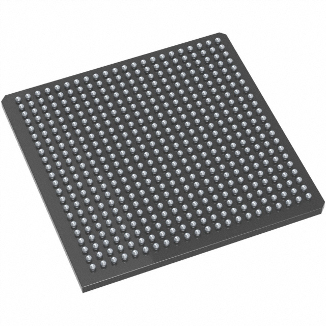
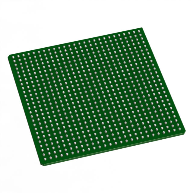
AX1000-FG676M
| Part Description |
Axcelerator Field Programmable Gate Array (FPGA) IC 418 165888 676-BGA |
|---|---|
| Quantity | 531 Available (as of June 15, 2026) |

| Product Category | Field Programmable Gate Array (FPGA) |
|---|---|
| Manufacturer | Microchip Technology |
| Manufacturing Status | Active |
| Manufacturer Standard Lead Time | 20 Weeks |
| Datasheet |
Specifications & Environmental
| Device Package | 676-FBGA (27x27) | Grade | Military | Operating Temperature | -55°C – 125°C | ||
|---|---|---|---|---|---|---|---|
| Package / Case | 676-BGA | Number of I/O | 418 | Voltage | 1.425 V - 1.575 V | ||
| Mounting Method | Surface Mount | RoHS Compliance | RoHS non-compliant | REACH Compliance | REACH Unaffected | ||
| Moisture Sensitivity Level | 3 (168 Hours) | Number of LABs/CLBs | 18144 | Number of Logic Elements/Cells | 18144 | ||
| Number of Gates | 1000000 | ECCN | 3A001A2C | HTS Code | 8542.39.0001 | ||
| Qualification | N/A | Total RAM Bits | 165888 |
Overview of AX1000-FG676M – Axcelerator FPGA IC with 418 I/Os, ~0.166 Mbits RAM, 676-BGA
The AX1000-FG676M is a high-performance Axcelerator field programmable gate array (FPGA) built on Microchip's AX architecture and antifuse CMOS process. It combines one million equivalent system gates, 18,144 logic elements, and embedded SRAM/FIFO resources to address demanding, secure, and military-grade designs.
Designed for applications that require high internal throughput, multi‑standard I/O support and nonvolatile programming, this device delivers deterministic timing, integrated PLLs and hardware features that simplify system-level integration while maintaining design security.
Key Features
- Core Performance — ~1,000,000 equivalent system gates and 18,144 logic elements provide substantial logic capacity for complex FPGA designs.
- Embedded Memory & FIFO — Approximately 165,888 bits (~0.166 Mbits) of embedded SRAM with programmable FIFO control logic and variable-aspect RAM blocks for flexible data buffering and storage.
- I/O Capability — 418 user I/Os with multi-standard support (single-ended and differential standards including LVDS and LVPECL), bank-selectable voltage operation and programmable slew/drive strength for mixed-voltage systems.
- High-Speed Clocking — Embedded PLLs and segmentable clock resources supporting wide input ranges and frequency synthesis for high-throughput internal and system clocks.
- Nonvolatile Security — Antifuse-based single-chip nonvolatile programming and FuseLock™ protection to guard against reverse engineering and protect intellectual property.
- Power & Supply — Core voltage range specified at 1.425 V to 1.575 V for optimized low-core-power operation.
- Package & Mounting — 676-ball fine BGA (676-FBGA, 27 × 27) surface-mount footprint suitable for dense board designs.
- Operating Range — Qualified for military-grade temperature operation from −55 °C to 125 °C.
- Design & Test Support — Deterministic, user-controllable timing, boundary-scan (JTAG) and in‑system diagnostic/debug capability via Microchip Silicon Explorer II.
- Standards & Configurability — Flexible I/O standards (1.5 V to 3.3 V operation, multiple voltage-referenced I/O types), registered I/Os, programmable input pull devices and hot-swap compliant I/Os (except PCI).
Typical Applications
- Defense & Military Electronics — Military-grade temperature range and nonvolatile antifuse programming make the AX1000-FG676M well suited for rugged, secure embedded systems.
- High-Speed Communications — High internal performance, embedded FIFOs and LVDS-capable I/Os support data-path implementations and protocol bridging in communications equipment.
- Secure Processing & IP Protection — Antifuse programming and FuseLock protection serve cryptographic modules, secure controllers and systems where design security is required.
- Deterministic Control Systems — Deterministic timing and integrated PLLs enable real-time control, timing-critical signal processing and hardware-accelerated functions.
Unique Advantages
- Highly integrated logic and memory: Combines 1,000,000 equivalent gates, 18,144 logic elements and ~0.166 Mbits of embedded SRAM to reduce external components and simplify BOM.
- Nonvolatile, tamper-resistant configuration: Antifuse technology and FuseLock protection provide one-time programmable, secure configuration that resists reverse engineering.
- Flexible, high-speed I/O: 418 user I/Os with support for multiple standards and programmable drive/slew options ease interface compatibility across subsystems.
- Military-temperature capability: −55 °C to 125 °C operating range and surface-mount 676-FBGA packaging support deployment in harsh environments.
- Deterministic timing and debug: User-controllable timing resources, embedded PLLs and in-system diagnostic/debug support streamline verification and system bring-up.
- Vendor tooling and test support: Boundary-scan (JTAG) compliance and Microchip diagnostic tools accelerate development and simplify production test.
Why Choose AX1000-FG676M?
The AX1000-FG676M positions itself as a robust, secure FPGA option for designs requiring substantial logic density, embedded memory/FIFO capability and multi-standard I/O flexibility under military-grade environmental conditions. Its antifuse, single-chip nonvolatile architecture and FuseLock protection provide a high level of IP security while integrated PLLs and deterministic timing address demanding performance needs.
This device is suited for systems engineers and procurement teams building secure, high-reliability designs where long-term stability, board-level density and proven diagnostic/test support are key considerations.
Request a quote or submit an inquiry to obtain pricing, lead times and availability for the AX1000-FG676M. Our team can provide the datasheet and technical assistance to evaluate this device for your design.


Date Founded: 1989
Headquarters: Chandler, Arizona, USA
Employees: 22,000+
Revenue: $8.349 Billion
Certifications and Memberships: ISO9001:2015, IATF16949:2016, AS 9100D


