
AX1000-FGG484
| Part Description |
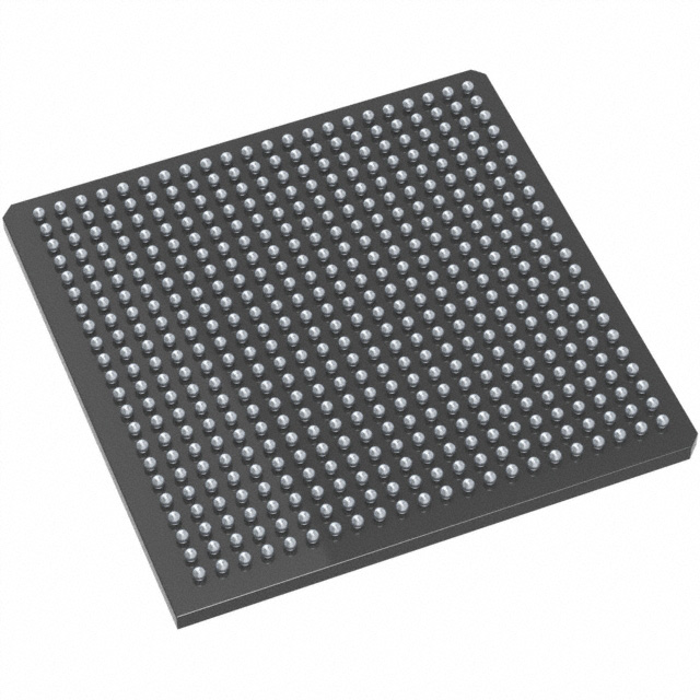
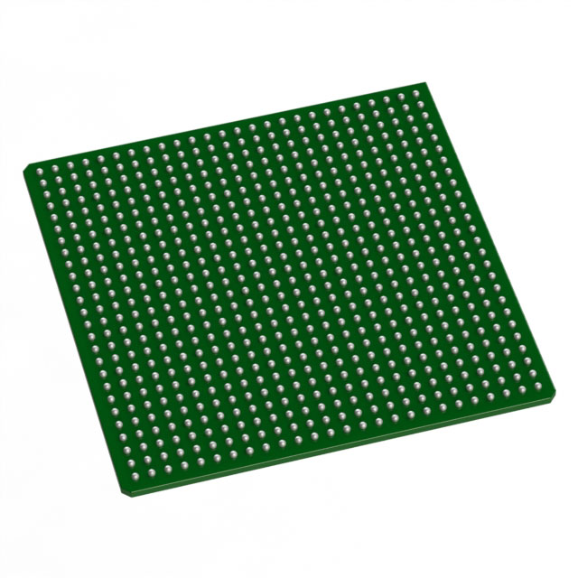
Axcelerator Field Programmable Gate Array (FPGA) IC 317 165888 484-BGA |
|---|---|
| Quantity | 815 Available (as of June 15, 2026) |

| Product Category | Field Programmable Gate Array (FPGA) |
|---|---|
| Manufacturer | Microchip Technology |
| Manufacturing Status | Active |
| Manufacturer Standard Lead Time | 12 Weeks |
| Datasheet |
Specifications & Environmental
| Device Package | 484-FPBGA (23x23) | Grade | Commercial | Operating Temperature | 0°C – 70°C | ||
|---|---|---|---|---|---|---|---|
| Package / Case | 484-BGA | Number of I/O | 317 | Voltage | 1.425 V - 1.575 V | ||
| Mounting Method | Surface Mount | RoHS Compliance | ROHS3 Compliant | REACH Compliance | REACH Unaffected | ||
| Moisture Sensitivity Level | 3 (168 Hours) | Number of LABs/CLBs | 18144 | Number of Logic Elements/Cells | 18144 | ||
| Number of Gates | 1000000 | ECCN | 3A001A7A | HTS Code | 8542.39.0001 | ||
| Qualification | N/A | Total RAM Bits | 165888 |
Overview of AX1000-FGG484 – Axcelerator FPGA, 317 I/Os, 165,888‑bit RAM, 484‑BGA
The AX1000-FGG484 is a Microchip Axcelerator-family Field Programmable Gate Array (FPGA) implemented on the AX architecture using a CMOS antifuse process. It delivers a single-chip, nonvolatile programmable logic solution with on-chip embedded memory and flexible multi-standard I/Os for demanding digital designs.
Designed for high-performance, security-conscious designs, the device combines substantial logic capacity, embedded SRAM/FIFO resources and high-speed I/O capability to support system-level functions such as clock synthesis, data buffering and deterministic timing control.
Key Features
- AX Architecture & Antifuse Technology Single-chip, nonvolatile antifuse FPGA architecture with FuseLock programming technology for design protection and secure, one-time programmable logic.
- Logic Resources Approximately 1,000,000 equivalent system gates and 18,144 logic elements (cells) to implement complex digital functions.
- Embedded Memory & FIFOs Total on-chip embedded memory of 165,888 bits arranged in core RAM blocks (family supports variable-aspect 4,608‑bit blocks) with embedded FIFO control logic for efficient data buffering.
- I/O Capacity & Standards 317 user I/Os with bank-selectable, mixed-voltage operation. Family-level I/O features include high-speed LVDS capable interfaces (up to 700 Mb/s) and support for single-ended and differential standards.
- Clocking & PLLs Segmentable clock resources and embedded PLLs for frequency synthesis (datasheet lists PLL input range 14–200 MHz and synthesis capability up to 1 GHz), enabling flexible timing architectures.
- Performance Family-level system and internal performance characteristics include 350+ MHz system performance and 500+ MHz internal performance for high-throughput logic implementations.
- Package & Mounting 484‑ball Fine-Pitch BGA (484‑FPBGA, 23 × 23) surface-mount package suited for compact, board-level integration.
- Power & Temperature Core supply voltage range 1.425 V to 1.575 V. Commercial-grade operating range from 0 °C to 70 °C.
- Compliance RoHS‑compliant construction for environmental regulatory alignment.
Typical Applications
- High-speed data interfaces — Implement LVDS and other differential serial links and on-chip FIFO buffering for robust, high-bandwidth data transfer.
- Secure programmable logic — Antifuse nonvolatile architecture and FuseLock programming provide protection against reverse engineering for IP-sensitive designs.
- Embedded system control — Use the device’s logic density, embedded memory and PLLs for deterministic control, protocol handling and system glue logic in complex embedded platforms.
- Custom ASIC replacement and prototyping — High gate count and abundant logic elements enable consolidation of multiple functions into a single programmable device for rapid design iterations.
Unique Advantages
- Nonvolatile, one-time programmable design: Antifuse technology yields a single-chip nonvolatile solution that eliminates the need for external configuration memory.
- Significant logic and memory density: ~1,000,000 equivalent system gates and approximately 165,888 bits of embedded memory support complex algorithms and substantial buffering on-chip.
- Flexible I/O and mixed-voltage banks: Bank-selectable I/Os and multi-standard support enable easy interfacing with a wide range of peripherals and voltage domains.
- High-performance clocking: Segmentable clocks and embedded PLLs provide precise timing control and on-chip frequency synthesis for high-speed designs.
- Security-oriented features: FuseLock programming protects intellectual property and reduces risks associated with reverse engineering.
- Compact board-level integration: 484‑ball FPBGA surface-mount package provides a high-density footprint for space-constrained PCBs.
Why Choose AX1000-FGG484?
The AX1000-FGG484 positions as a high-density, nonvolatile FPGA aimed at designs that require substantial logic capacity, embedded memory and secure programmable logic. Its combination of AX antifuse architecture, embedded FIFOs, PLL-based clocking and flexible I/Os makes it well suited for engineers implementing high-speed interfaces, complex control logic and IP-protected designs.
For development teams and procurement decision-makers seeking a compact, single-chip programmable solution with verifiable specifications for voltage, temperature and package, the AX1000-FGG484 offers a clear match between system-level capability and deterministic, in-system behavior backed by Microchip’s Axcelerator family documentation.
Request a quote or submit an inquiry to discuss availability, pricing and lead times for the AX1000-FGG484.


Date Founded: 1989
Headquarters: Chandler, Arizona, USA
Employees: 22,000+
Revenue: $8.349 Billion
Certifications and Memberships: ISO9001:2015, IATF16949:2016, AS 9100D


