
AX1000-2FGG484
| Part Description |
Axcelerator Field Programmable Gate Array (FPGA) IC 317 165888 484-BGA |
|---|---|
| Quantity | 1,395 Available (as of June 15, 2026) |
| Product Category | Field Programmable Gate Array (FPGA) |
|---|---|
| Manufacturer | Microchip Technology |
| Manufacturing Status | Active |
| Manufacturer Standard Lead Time | 12 Weeks |
| Datasheet |
Specifications & Environmental
| Device Package | 484-FPBGA (23x23) | Grade | Commercial | Operating Temperature | 0°C – 70°C | ||
|---|---|---|---|---|---|---|---|
| Package / Case | 484-BGA | Number of I/O | 317 | Voltage | 1.425 V - 1.575 V | ||
| Mounting Method | Surface Mount | RoHS Compliance | ROHS3 Compliant | REACH Compliance | REACH Unaffected | ||
| Moisture Sensitivity Level | 3 (168 Hours) | Number of LABs/CLBs | 18144 | Number of Logic Elements/Cells | 18144 | ||
| Number of Gates | 1000000 | ECCN | 3A001A7A | HTS Code | 8542.39.0001 | ||
| Qualification | N/A | Total RAM Bits | 165888 |
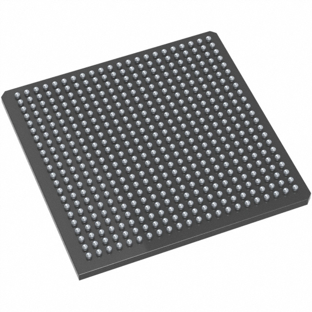
Overview of AX1000-2FGG484 – Axcelerator Field Programmable Gate Array (FPGA), 1,000,000 gates, 317 I/Os, 484‑BGA
The AX1000-2FGG484 from Microchip Technology is an Axcelerator antifuse FPGA built on the AX architecture. This single-chip, nonvolatile FPGA delivers 1,000,000 equivalent system gates, 18,144 logic elements and embedded memory suitable for commercial-temperature designs.
Designed for high-performance digital systems, the device addresses designs that require deterministic timing, embedded FIFOs and flexible multi-standard I/O support while operating from a 1.425 V to 1.575 V core supply and a 0 °C to 70 °C commercial temperature range.
Key Features
- Core & Logic 1,000,000 equivalent system gates and 18,144 logic elements provide substantial combinatorial and registered resources for complex logic implementations.
- Embedded Memory & FIFOs Approximately 0.166 Mbits of embedded RAM (165,888 bits) organized in multiple core RAM blocks with programmable FIFO control logic for buffering and data flow management.
- I/O Flexibility 317 user I/Os with support for multi-voltage operation (1.5 V, 1.8 V, 2.5 V, 3.3 V) and differential standards such as LVDS and LVPECL as described in the Axcelerator family documentation.
- Performance & Clocking Family-level capabilities include segmentable clocks and embedded PLLs with frequency synthesis enabling high internal and system performance.
- Security & Nonvolatile Programming Antifuse-based single-chip nonvolatile architecture and FuseLock programming technology protect design IP and prevent reverse engineering.
- Package & Mounting 484-ball Fine-Pitch BGA (484‑FPBGA, 23×23) surface-mount package suitable for compact PCB implementations.
- Power & Operating Range Core supply range 1.425 V to 1.575 V; commercial operating temperature 0 °C to 70 °C.
- Diagnostics & Test Supports boundary-scan testing compliant with IEEE 1149.1 (JTAG) and in-system diagnostic capability with Microchip Silicon Explorer II (family feature).
Typical Applications
- High‑speed communications Use the device’s LVDS-capable I/Os and embedded FIFOs for front-end interface logic, protocol bridging and line-rate data buffering.
- Signal processing and data aggregation Large logic and embedded memory resources enable complex data path implementations and on-chip buffering for real‑time processing.
- Secure, single‑chip systems Antifuse nonvolatile architecture and FuseLock programming provide hardware-level protection for security-conscious designs.
- Prototyping and volume ASIC replacement High gate capacity and deterministic timing resources allow consolidation of multiple functions into a single programmable device for compact system designs.
Unique Advantages
- Highly integrated resource set: 1,000,000 gates, 18,144 logic elements and embedded RAM reduce external components and simplify PCB designs.
- Nonvolatile antifuse technology: Single‑chip nonvolatile configuration removes the need for external configuration memory and enhances design security with FuseLock.
- Flexible I/O standards: Bank-selectable, multi-voltage I/O support and differential standards allow the AX1000 to interface with a wide range of peripherals and transceivers.
- Deterministic timing and on-chip PLLs: Segmentable clocks and embedded PLLs enable controlled timing architectures and frequency synthesis for complex timing requirements.
- Compact BGA package: 484‑ball FPBGA (23×23) provides high pin density in a compact footprint for space-constrained applications.
Why Choose AX1000-2FGG484?
The AX1000-2FGG484 positions itself as a high-capacity, nonvolatile FPGA for commercial-temperature systems that require significant logic density, embedded memory and flexible I/O. Its antifuse architecture and FuseLock programming deliver long-term configuration stability and design security while embedded PLLs, FIFOs and segmentable clocks support demanding timing and throughput requirements.
This device is suited for engineers and system designers consolidating functions into a single programmable device, implementing secure hardware features, or building high-performance communication and signal-processing subsystems where deterministic behavior and on-chip buffering matter.
Request a quote or submit an inquiry to receive pricing, availability and technical support information for the AX1000-2FGG484.


Date Founded: 1989
Headquarters: Chandler, Arizona, USA
Employees: 22,000+
Revenue: $8.349 Billion
Certifications and Memberships: ISO9001:2015, IATF16949:2016, AS 9100D


