
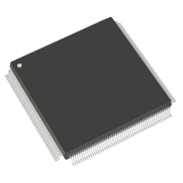
AX250-1PQ208M
| Part Description |
Axcelerator Field Programmable Gate Array (FPGA) IC 115 55296 208-BFQFP |
|---|---|
| Quantity | 225 Available (as of June 15, 2026) |
| Product Category | Field Programmable Gate Array (FPGA) |
|---|---|
| Manufacturer | Microchip Technology |
| Manufacturing Status | Obsolete |
| Manufacturer Standard Lead Time | Contact Us |
| Datasheet |
Specifications & Environmental
| Device Package | 208-PQFP (28x28) | Grade | Military | Operating Temperature | -55°C – 125°C | ||
|---|---|---|---|---|---|---|---|
| Package / Case | 208-BFQFP | Number of I/O | 115 | Voltage | 1.425 V - 1.575 V | ||
| Mounting Method | Surface Mount | RoHS Compliance | RoHS non-compliant | REACH Compliance | REACH Unaffected | ||
| Moisture Sensitivity Level | 3 (168 Hours) | Number of LABs/CLBs | 4224 | Number of Logic Elements/Cells | 4224 | ||
| Number of Gates | 250000 | ECCN | 3A001A2C | HTS Code | 8542.39.0001 | ||
| Qualification | N/A | Total RAM Bits | 55296 |
Overview of AX250-1PQ208M – Axcelerator Field Programmable Gate Array (FPGA) IC 115 55296 208-BFQFP
The AX250-1PQ208M is a Microchip Technology Axcelerator antifuse FPGA based on the AX architecture and a 0.15 µm CMOS antifuse process with seven layers of metal. This nonvolatile, single-chip solution delivers deterministic timing, embedded SRAM/FIFO control logic and flexible, multi-standard I/Os for high-performance embedded and mission-critical designs.
Designed for applications requiring secure configuration, high-speed I/O and wide operating range, the device combines 250,000 equivalent system gates with 4,224 logic elements and approximately 55,296 bits of embedded RAM to enable complex logic integration and on-chip buffering.
Key Features
- Core & Architecture AX antifuse architecture implemented in 0.15 µm CMOS with seven metal layers, providing a single-chip, nonvolatile FPGA solution and deterministic, user-controllable timing.
- Logic Resources 250,000 equivalent system gates and 4,224 logic elements (cells) suitable for substantial combinatorial and registered logic integration.
- Embedded Memory & FIFOs 55,296 bits of embedded SRAM with embedded FIFO control logic and variable-aspect RAM blocks for configurable width and porting options.
- I/O Flexibility 115 user I/Os with support for multi-voltage banks, differential standards including LVDS and LVPECL, and programmable slew rate, drive strength and input pull circuits.
- Performance System performance up to 350+ MHz, internal performance up to 500+ MHz, and LVDS-capable I/Os up to 700 Mb/s as documented for the Axcelerator family.
- Clocking & PLLs Segmentable clock resources and embedded PLLs with 14–200 MHz input range and frequency synthesis capabilities up to 1 GHz.
- Power & Voltage 1.425 V to 1.575 V core supply range (nominal 1.5 V core operation) for low-power core operation.
- Package & Mounting Surface-mount PQFP package: 208-BFQFP (supplier device package 208-PQFP, 28 × 28 mm).
- Temperature & Grade Military grade with operating temperature range of –55 °C to 125 °C.
- Security & Test FuseLock programming technology to protect against reverse engineering and design theft; JTAG boundary-scan testing (IEEE 1149.1) supported.
- Compliance RoHS compliant.
Typical Applications
- High-speed data acquisition Use embedded FIFOs, high-performance internal logic and LVDS-capable I/Os to aggregate and buffer multi-channel, high-rate data streams.
- Telecommunications and networking Implement protocol bridging, packet processing and timing-sensitive functions leveraging segmentable clocks, PLL frequency synthesis and deterministic timing.
- Military and aerospace systems Military-grade temperature range and nonvolatile antifuse configuration provide robustness and secure configuration for deployable and rugged applications.
- Real-time signal processing Combine abundant logic elements and on-chip RAM/FIFO resources to implement deterministic, low-latency DSP pipelines and custom accelerators.
Unique Advantages
- Nonvolatile, secure configuration: Antifuse single-chip programming with FuseLock protects IP and prevents reverse engineering.
- Deterministic timing and performance: Segmentable clocks, user-controllable timing and PLLs provide predictable timing for real-time systems.
- High-performance I/O capability: LVDS-capable I/Os to 700 Mb/s and multi-standard bank-selectable I/O support a wide range of interface standards.
- Embedded buffering and memory: On-chip SRAM with embedded FIFO control simplifies data flow design and reduces external memory dependence.
- Rugged operating range: Military grade and –55 °C to 125 °C operation enable designs for harsh environmental conditions.
- Compact, surface-mount package: 208-BFQFP (208-PQFP 28 × 28 mm) supports dense PCB integration while preserving I/O count and thermal performance.
Why Choose AX250-1PQ208M?
The AX250-1PQ208M positions itself as a high-performance, secure and robust FPGA option for applications that require deterministic timing, on-chip memory/FIFO resources and flexible, high-speed I/O. With 250,000 equivalent system gates, 4,224 logic elements and approximately 55,296 bits of embedded RAM, it enables complex logic and data buffering on a single nonvolatile device.
Engineers designing telecommunications, high-speed data acquisition, real-time signal processing or military/aerospace systems will benefit from the Axcelerator family’s programmable clocks and PLLs, LVDS-capable I/Os, wide temperature range and built-in security features—providing long-term design stability and IP protection backed by Microchip’s Axcelerator architecture.
Request a quote or submit a product inquiry to receive pricing and availability information for the AX250-1PQ208M.


Date Founded: 1989
Headquarters: Chandler, Arizona, USA
Employees: 22,000+
Revenue: $8.349 Billion
Certifications and Memberships: ISO9001:2015, IATF16949:2016, AS 9100D


