
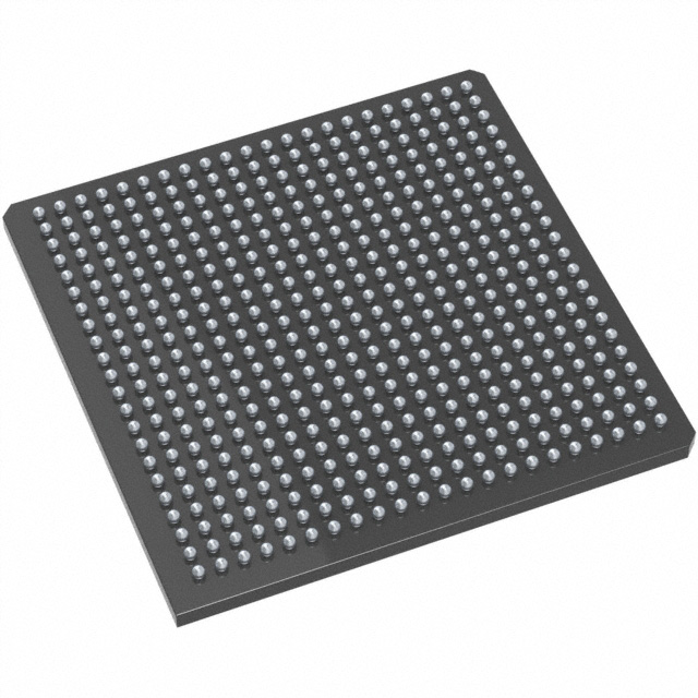
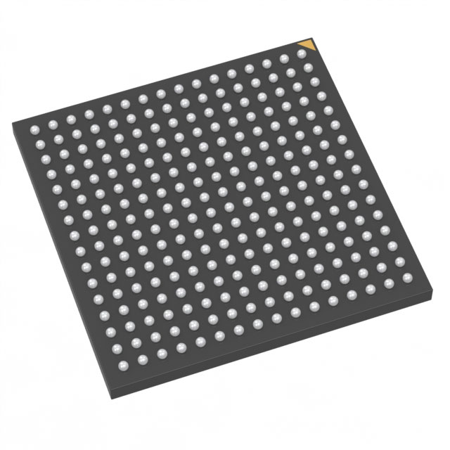
AX250-2FG484
| Part Description |
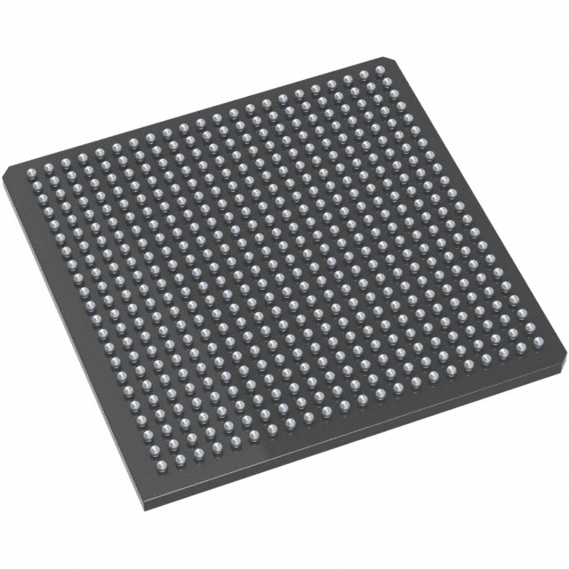
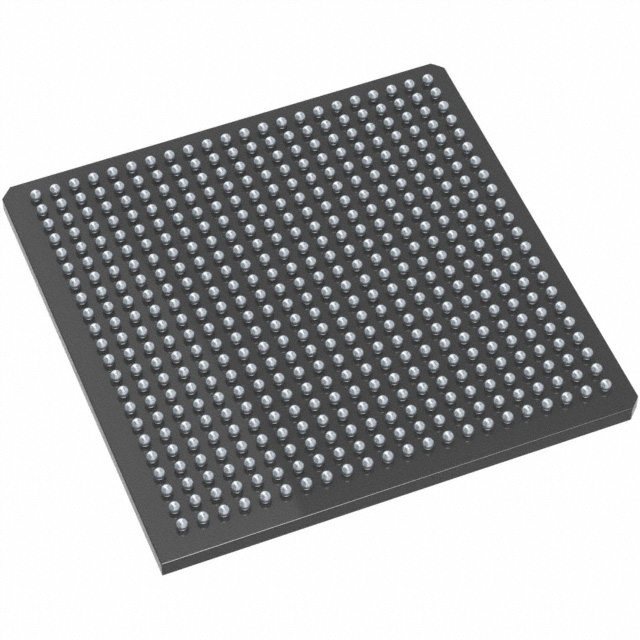
Axcelerator Field Programmable Gate Array (FPGA) IC 248 55296 484-BGA |
|---|---|
| Quantity | 125 Available (as of October 8, 2026) |
| Product Category | Field Programmable Gate Array (FPGA) |
|---|---|
| Manufacturer | Microchip Technology |
| Manufacturing Status | Active |
| Manufacturer Standard Lead Time | 8 Weeks |
| Datasheet |
Specifications & Environmental
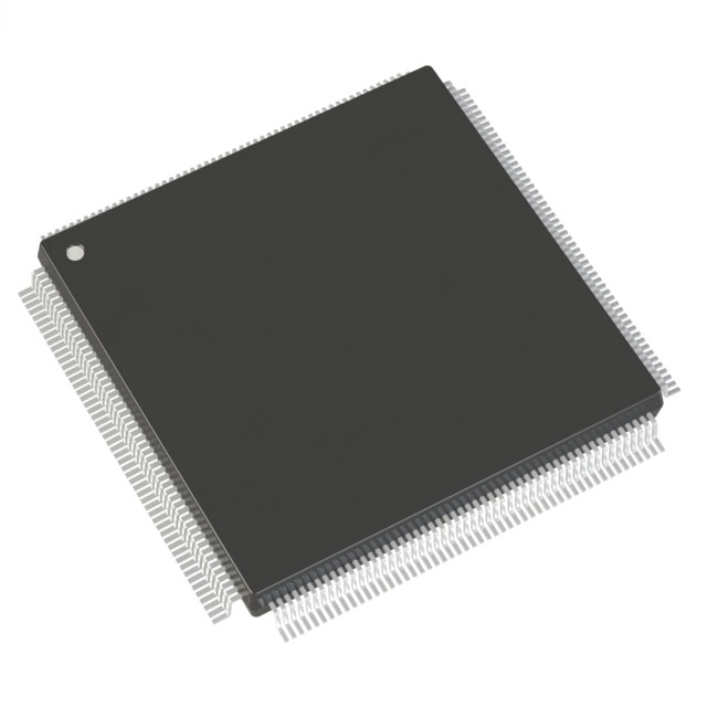
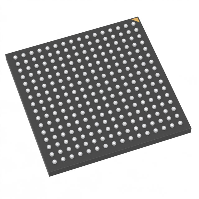
| Device Package | 484-FPBGA (23x23) | Grade | Commercial | Operating Temperature | 0°C – 70°C | ||
|---|---|---|---|---|---|---|---|
| Package / Case | 484-BGA | Number of I/O | 248 | Voltage | 1.425 V - 1.575 V | ||
| Mounting Method | Surface Mount | RoHS Compliance | RoHS non-compliant | REACH Compliance | REACH Unaffected | ||
| Moisture Sensitivity Level | 3 (168 Hours) | Number of LABs/CLBs | 4224 | Number of Logic Elements/Cells | 4224 | ||
| Number of Gates | 250000 | ECCN | 3A991D | HTS Code | 8542.39.0001 | ||
| Qualification | N/A | Total RAM Bits | 55296 |
Overview of AX250-2FG484 – Axcelerator FPGA, 250k gates, 248 I/Os, 484-BGA
The AX250-2FG484 is an Axcelerator family Field Programmable Gate Array (FPGA) from Microchip Technology based on the AX architecture and antifuse CMOS process. This commercial-grade, single-chip nonvolatile solution delivers 250,000 equivalent system gates, 4,224 logic elements and 55,296 bits of embedded SRAM/FIFO, targeted at high-performance embedded and communications designs that require deterministic timing, on-chip memory and flexible I/O.
Designed for surface-mount applications, the device is supplied in a 484-ball FPBGA (23×23) package and operates from a core supply range of 1.425 V to 1.575 V with an operating temperature range of 0 °C to 70 °C. It is RoHS compliant and includes family-level features such as segmentable clocks, PLLs and security-oriented programming.
Key Features
- Core Capacity and Logic — 250,000 equivalent system gates with 4,224 logic elements for implementing mid-range to complex logic functions.
- Embedded Memory & FIFOs — 55,296 bits of embedded SRAM/FIFO and high-performance embedded FIFO control logic for buffering and streaming data on-chip.
- I/O Density and Standards — 248 user I/Os with multi-standard support in the Axcelerator family, including LVDS-capable channels (700 Mb/s mentioned at the family level) and bank-selectable mixed-voltage operation.
- Performance — Family-level performance indicators include 350+ MHz system performance and 500+ MHz internal performance, enabling high-speed datapaths and logic operation.
- Clocking and PLL — Segmentable clock resources and embedded PLLs with a 14–200 MHz input range and frequency synthesis capabilities up to 1 GHz (family-level specification).
- Nonvolatile Antifuse Technology & Security — Single-chip, nonvolatile antifuse programming and FuseLock™ programming technology to protect against reverse engineering and design theft (family-level features).
- Power — Core supply range centered around 1.5 V (1.425 V to 1.575 V) to support low-power core operation.
- Package & Mounting — Surface-mount 484-BGA package (484-FPBGA, 23×23 footprint) suitable for compact board-level integration.
- Compliance & Testing — Boundary-scan testing compliant with IEEE 1149.1 (JTAG) and RoHS-compliant manufacturing.
Typical Applications
- High-speed Communications — Use the device's high I/O count and LVDS-capable interfaces for serializers, protocol bridges and line-rate packet processing.
- Embedded Signal Processing — Implement DSP pipelines and hardware-accelerated processing using the device's 250k-gate capacity, internal RAM and high internal performance.
- System Control and Timing — Leverage segmentable clocks, deterministic timing and on-chip PLLs for precision timing, synchronization and control logic in embedded systems.
- Custom Hardware Acceleration — Create application-specific accelerators (offload engines, protocol handlers) using the combination of logic elements and embedded FIFOs to improve throughput and latency.
Unique Advantages
- Single-chip Nonvolatile Solution: Antifuse-based programming provides nonvolatile on-chip configuration, eliminating the need for external configuration memory.
- Deterministic, High-performance Timing: Segmentable clocks and embedded PLLs support stable, user-controllable timing suitable for high-speed datapaths.
- Flexible I/O and Mixed-Voltage Support: Bank-selectable I/Os and multiple supported standards enable integration with a wide range of interfaces and voltage domains.
- Embedded FIFO and Memory Resources: On-chip SRAM blocks and programmable FIFO control simplify buffering and dataflow management without external RAM.
- Security and IP Protection: FuseLock™ programming technology and nonvolatile antifuse architecture reduce the risk of reverse engineering and protect design IP.
- Proven Ecosystem Support: Family-level in-system diagnostic and debug capability with Microchip Silicon Explorer II provides development and test support.
Why Choose AX250-2FG484?
The AX250-2FG484 combines mid-range logic capacity, substantial on-chip memory and a high I/O count in a compact 484-BGA package, making it well suited for commercial embedded designs that demand deterministic timing, on-chip buffering and security. As part of Microchip's Axcelerator antifuse family, it benefits from family-level capabilities such as segmentable clocks, embedded PLLs and FuseLock programming for IP protection.
Choose the AX250-2FG484 when you need a surface-mount, nonvolatile FPGA solution with 250k equivalent gates, 4,224 logic elements and 55,296 bits of embedded memory for high-performance communication, processing and control applications in commercial temperature environments.
Request a quote or submit an RFQ for AX250-2FG484 to receive pricing, availability and ordering information.





















Date Founded: 1989
Headquarters: Chandler, Arizona, USA
Employees: 22,000+
Revenue: $8.349 Billion
Certifications and Memberships: ISO9001:2015, IATF16949:2016, AS 9100D




