
AX250-2FG484I
| Part Description |
Axcelerator Field Programmable Gate Array (FPGA) IC 248 55296 484-BGA |
|---|---|
| Quantity | 134 Available (as of June 15, 2026) |

| Product Category | Field Programmable Gate Array (FPGA) |
|---|---|
| Manufacturer | Microchip Technology |
| Manufacturing Status | Active |
| Manufacturer Standard Lead Time | 8 Weeks |
| Datasheet |
Specifications & Environmental
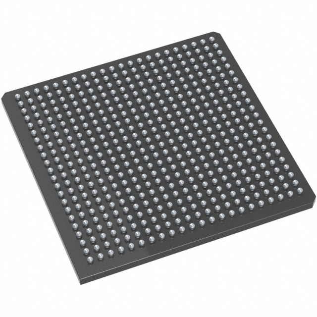
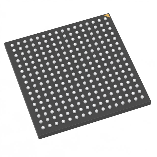
| Device Package | 484-FPBGA (23x23) | Grade | Industrial | Operating Temperature | -40°C – 85°C | ||
|---|---|---|---|---|---|---|---|
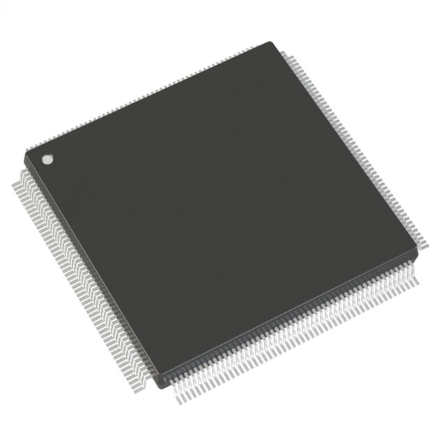
| Package / Case | 484-BGA | Number of I/O | 248 | Voltage | 1.425 V - 1.575 V | ||
| Mounting Method | Surface Mount | RoHS Compliance | RoHS non-compliant | REACH Compliance | REACH Unaffected | ||
| Moisture Sensitivity Level | 3 (168 Hours) | Number of LABs/CLBs | 4224 | Number of Logic Elements/Cells | 4224 | ||
| Number of Gates | 250000 | ECCN | 3A991D | HTS Code | 8542.39.0001 | ||
| Qualification | N/A | Total RAM Bits | 55296 |
Overview of AX250-2FG484I – Axcelerator Field Programmable Gate Array (FPGA) IC 248 I/Os 55,296 bits 484-BGA
The AX250-2FG484I is an Axcelerator family antifuse FPGA implementing Microchip’s AX architecture. It provides a nonvolatile, single-chip FPGA solution with substantial logic capacity, embedded memory and flexible I/O to address demanding industrial and high-performance embedded applications.
Designed for system-level integration, the device combines 250,000 equivalent system gates with segmentable clocks, embedded SRAM/FIFO control logic and multiple PLLs to support high-speed data paths and deterministic timing in industrial environments.
Key Features
- Core Capacity
Approximately 250,000 equivalent system gates with 4,224 logic elements, providing significant programmable logic for complex designs. - Embedded Memory
Approximately 55 kbits (55,296 bits) of on-chip RAM with FIFO control logic and variable-aspect RAM block organizations for flexible data buffering. - I/O and Interface Flexibility
248 user I/Os with LVDS-capable channels (700 Mb/s capability noted in the family data) and bank-selectable, multi-voltage operation to support mixed-voltage designs. - Clocking and PLLs
Segmentable clock resources and multiple embedded PLLs (family-level PLL features include a 14–200 MHz input range and frequency synthesis capabilities) for precise clock management and high-speed internal operation. - Performance
Family-level performance guidance cites system performance above 350 MHz and internal performance above 500 MHz to support fast data-path implementations. - Power and Core Voltage
Core supply range 1.425 V to 1.575 V (typical 1.5 V core), enabling low-voltage operation consistent with the Axcelerator architecture. - Package and Mounting
484-ball fine-pitch BGA (484-FPBGA, 23 × 23) in a surface-mount package for compact board-level integration. - Industrial Grade Temperature
Rated for operation from −40 °C to 85 °C to meet industrial environment requirements. - Design Security and Testability
Antifuse-based, nonvolatile programming with family features such as FuseLock programming and JTAG boundary-scan support for diagnostics and IP protection. - Compliance
RoHS compliant.
Typical Applications
- High-speed data interfaces — Use LVDS-capable I/Os and embedded FIFOs to implement multi-channel, high-throughput serial links and data aggregation.
- Industrial control and automation — Industrial-grade temperature range and robust I/O support enable motor control, sensor aggregation and real-time control logic in factory equipment.
- Protocol bridging and interface consolidation — Mixed-voltage, bank-selectable I/Os allow consolidation of multiple legacy and modern interfaces within a single FPGA fabric.
- Custom embedded processing — Significant logic and embedded memory resources support application-specific accelerators, preprocessing and deterministic system control.
Unique Advantages
- Single-chip, nonvolatile solution: Antifuse-based FPGA provides permanent configuration storage without external configuration memory, simplifying system BOM and boot sequencing.
- Substantial programmable capacity: 250,000 equivalent gates and 4,224 logic elements deliver headroom for complex state machines, datapaths and control logic.
- Flexible, high-speed I/O: 248 I/Os with LVDS capability and multi-standard support allow direct interfacing to high-speed links and mixed-voltage peripherals.
- Deterministic timing and clock control: Segmentable clocks and multiple PLLs enable controlled timing domains and stable, high-frequency internal operation.
- Industrial-ready packaging and thermal range: 484-BGA surface-mount package and −40 °C to 85 °C rating meet common industrial deployment requirements.
Why Choose AX250-2FG484I?
The AX250-2FG484I positions itself as a high-capacity, industrial-grade antifuse FPGA aimed at designers who need a compact, nonvolatile programmable logic device with strong I/O flexibility and on-chip memory. Its combination of 250k equivalent gates, thousands of logic elements, embedded SRAM/FIFO resources and robust clocking support makes it suitable for systems requiring deterministic timing, secure programming and high-speed interfacing.
For teams building industrial automation, high-speed data transport, protocol conversion or custom embedded acceleration, this device delivers integrated resources that reduce external components and simplify system architecture while providing long-term deployment stability and RoHS compliance.
Request a quote or submit a purchase inquiry to learn about availability, lead times and packaging options for AX250-2FG484I. Our team can provide pricing and configuration guidance for your design requirements.


Date Founded: 1989
Headquarters: Chandler, Arizona, USA
Employees: 22,000+
Revenue: $8.349 Billion
Certifications and Memberships: ISO9001:2015, IATF16949:2016, AS 9100D


