
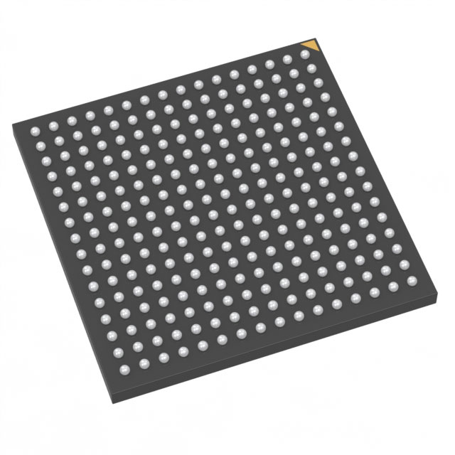
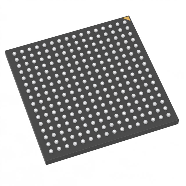
AX250-2FG256
| Part Description |
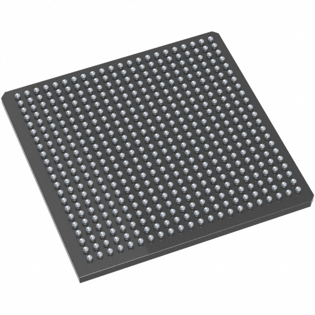
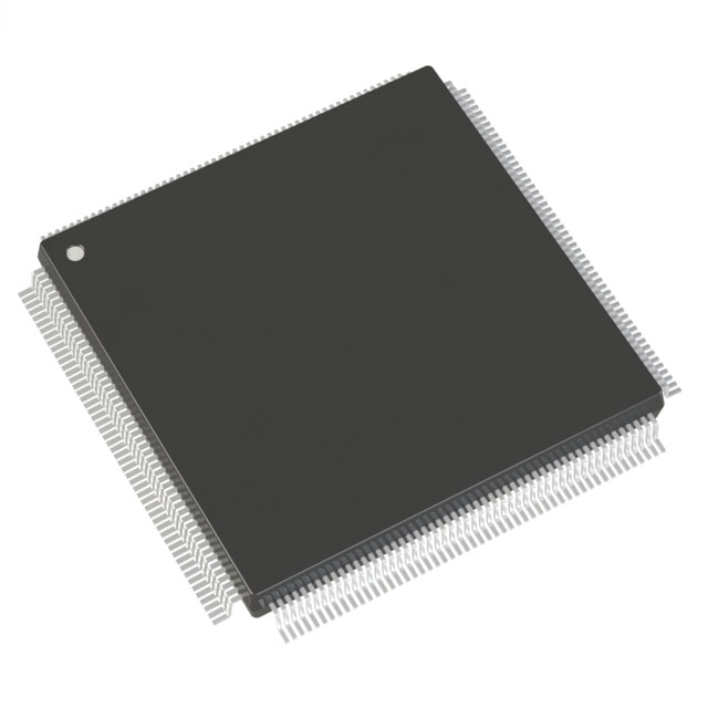
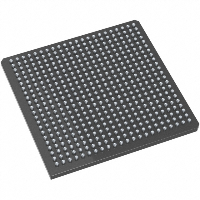
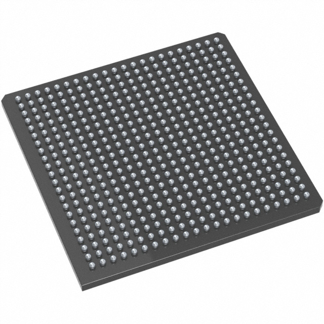
Axcelerator Field Programmable Gate Array (FPGA) IC 138 55296 256-LBGA |
|---|---|
| Quantity | 50 Available (as of October 8, 2026) |
| Product Category | Field Programmable Gate Array (FPGA) |
|---|---|
| Manufacturer | Microchip Technology |
| Manufacturing Status | Active |
| Manufacturer Standard Lead Time | 8 Weeks |
| Datasheet |
Specifications & Environmental
| Device Package | 256-FPBGA (17x17) | Grade | Commercial | Operating Temperature | 0°C – 70°C | ||
|---|---|---|---|---|---|---|---|
| Package / Case | 256-LBGA | Number of I/O | 138 | Voltage | 1.425 V - 1.575 V | ||
| Mounting Method | Surface Mount | RoHS Compliance | RoHS non-compliant | REACH Compliance | REACH Unaffected | ||
| Moisture Sensitivity Level | 3 (168 Hours) | Number of LABs/CLBs | 4224 | Number of Logic Elements/Cells | 4224 | ||
| Number of Gates | 250000 | ECCN | 3A991D | HTS Code | 8542.39.0001 | ||
| Qualification | N/A | Total RAM Bits | 55296 |
Overview of AX250-2FG256 – Axcelerator FPGA, 250k gates, 138 I/Os, 256-LBGA
The AX250-2FG256 is an Axcelerator Field Programmable Gate Array (FPGA) from Microchip Technology based on the AX antifuse architecture. It delivers 250,000 equivalent system gates with 4,224 logic elements and integrated resources designed for high-performance, deterministic programmable logic applications.
Targeted at commercial designs, this surface-mount 256-LBGA device combines embedded SRAM/FIFO control logic, bank-selectable mixed-voltage I/Os and on-chip PLLs to address high-speed data, control and embedded processing use cases where reproducible timing and in-system programmability are required.
Key Features
- Core Architecture AX antifuse architecture manufactured on 0.15 μm CMOS with seven metal layers, providing a single-chip, nonvolatile solution and deterministic timing characteristics.
- Capacity & Logic 250,000 equivalent system gates and 4,224 logic elements (cells) to implement medium-density programmable logic designs.
- Embedded Memory & FIFOs Approximately 55 kbits of embedded SRAM/FIFO (55,296 bits total) with variable-aspect 4,608-bit RAM blocks and programmable FIFO control logic.
- I/O Flexibility 138 user I/Os with bank-selectable mixed-voltage operation (1.5V, 1.8V, 2.5V, 3.3V), programmable slew rate and drive strength, and up to 700 Mb/s LVDS-capable I/Os.
- Clocking & PLLs Segmentable clock resources plus embedded PLLs supporting 14–200 MHz inputs and frequency synthesis capabilities up to 1 GHz.
- Performance System performance up to 350+ MHz and internal performance up to 500+ MHz as documented for the Axcelerator family.
- Power & Supply Core voltage supply range specified at 1.425 V to 1.575 V (nominal 1.5V core voltage for low power operation).
- Package & Mechanical 256-LBGA package (supplier device package: 256-FPBGA, 17 × 17 mm) for surface-mount assembly; RoHS-compliant.
- Operating Grade Commercial grade device with an operating temperature range of 0 °C to 70 °C.
- Security & Test FuseLock programming technology for protection against reverse engineering, plus IEEE 1149.1 (JTAG) boundary-scan support and in-system diagnostic capability with Microchip Silicon Explorer II.
Typical Applications
- High-performance embedded systems Implement medium-density custom logic and control functions where deterministic timing and on-chip memory/FIFO support are required.
- High-speed I/O interfaces Use the LVDS-capable I/Os and programmable I/O standards for serial data links and protocol bridging up to 700 Mb/s.
- Data buffering and packet processing Leverage embedded SRAM/FIFO blocks and high internal clock performance for packet buffering, queuing and flow control.
- Custom accelerator logic Deploy application-specific datapaths or hardware accelerators using the 4,224 logic elements and up to 250k gates of capacity.
Unique Advantages
- Single-chip nonvolatile configuration: Antifuse-based programming provides a one-time nonvolatile configuration that simplifies system boot and removes the need for external configuration memory.
- Deterministic, high-speed operation: Documented system and internal clock performance (350+ MHz system, 500+ MHz internal) supports time-sensitive designs.
- Integrated memory and FIFO control: On-chip SRAM/FIFO blocks reduce external memory requirements and simplify board-level BOM for buffering and streaming applications.
- Flexible I/O standards: Bank-selectable mixed-voltage I/Os and programmable output characteristics enable interfacing to a wide range of system peripherals without extra level-shifting components.
- Design security and testability: FuseLock programming and IEEE 1149.1 boundary-scan support help protect IP and streamline manufacturing test and in-system diagnostics.
- Tool-supported in-system debug: In-system diagnostic capability with Microchip Silicon Explorer II facilitates development and fault isolation.
Why Choose AX250-2FG256?
The AX250-2FG256 positions itself as a compact, medium-density Axcelerator FPGA offering a balanced combination of logic capacity (250k gates, 4,224 logic elements), integrated memory (≈55 kbits) and flexible, high-speed I/Os in a 256-LBGA surface-mount package. Its antifuse, single-chip nonvolatile architecture and deterministic timing characteristics make it well suited for commercial embedded designs that require reproducible performance and in-system diagnostics.
Designers seeking an FPGA with built-in FIFO control, embedded PLLs and robust I/O flexibility will find the AX250-2FG256 a practical choice for reducing external components, simplifying board design and accelerating time-to-market while leveraging Microchip’s diagnostic tool support.
Request a quote or submit an inquiry for pricing and availability for the AX250-2FG256 to evaluate it for your next design.





















Date Founded: 1989
Headquarters: Chandler, Arizona, USA
Employees: 22,000+
Revenue: $8.349 Billion
Certifications and Memberships: ISO9001:2015, IATF16949:2016, AS 9100D




