
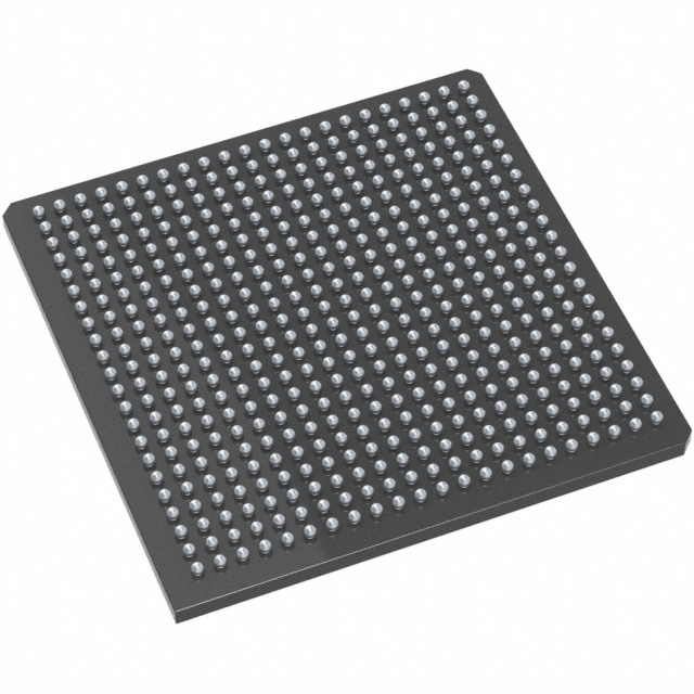
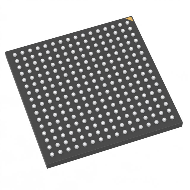
AX250-2FGG484
| Part Description |
Axcelerator Field Programmable Gate Array (FPGA) IC 248 55296 484-BGA |
|---|---|
| Quantity | 1,426 Available (as of June 15, 2026) |

| Product Category | Field Programmable Gate Array (FPGA) |
|---|---|
| Manufacturer | Microchip Technology |
| Manufacturing Status | Active |
| Manufacturer Standard Lead Time | 8 Weeks |
| Datasheet |
Specifications & Environmental
| Device Package | 484-FPBGA (23x23) | Grade | Commercial | Operating Temperature | 0°C – 70°C | ||
|---|---|---|---|---|---|---|---|
| Package / Case | 484-BGA | Number of I/O | 248 | Voltage | 1.425 V - 1.575 V | ||
| Mounting Method | Surface Mount | RoHS Compliance | ROHS3 Compliant | REACH Compliance | REACH Unaffected | ||
| Moisture Sensitivity Level | 3 (168 Hours) | Number of LABs/CLBs | 4224 | Number of Logic Elements/Cells | 4224 | ||
| Number of Gates | 250000 | ECCN | 3A991D | HTS Code | 8542.39.0001 | ||
| Qualification | N/A | Total RAM Bits | 55296 |
Overview of AX250-2FGG484 – Axcelerator FPGA, 248 I/O, 484-BGA
The AX250-2FGG484 is an Axcelerator Field Programmable Gate Array (FPGA) from Microchip Technology based on the AX architecture and CMOS antifuse process. It delivers a nonvolatile, single-chip FPGA solution with 250,000 equivalent system gates and 4,224 logic elements, targeting commercial applications that require high I/O density, embedded memory, and deterministic timing.
Configured in a 484-ball fine-pitch BGA (484-FPBGA, 23×23) surface-mount package, the device provides 248 user I/Os, on-chip embedded SRAM/FIFO (55,296 bits), segmentable clock resources and embedded PLLs, and operates from a 1.425 V to 1.575 V core supply at commercial temperature range (0 °C to 70 °C). The device is RoHS compliant.
Key Features
- Core & Architecture AX architecture with a nonvolatile CMOS antifuse implementation delivering 250,000 equivalent gates and 4,224 logic elements for system-level integration.
- Memory & FIFO Approximately 55,296 bits of embedded SRAM organized in core RAM blocks with programmable FIFO control logic to support buffering and width-configurable ports.
- I/O Flexibility 248 user I/Os with bank-selectable configurations (up to 8 I/O banks), programmable slew rate and drive strength, and support for multiple single-ended and differential standards including LVDS capable to 700 Mb/s.
- Clocking & Timing Segmentable clock resources and embedded phase-locked loops (PLLs) with a 14–200 MHz input range and frequency synthesis capabilities up to 1 GHz for precision clocking and timing control.
- Performance System-level performance characteristics include 350+ MHz system performance and 500+ MHz internal performance for demanding timing requirements.
- Security & Nonvolatile Programming Antifuse-based nonvolatile programming with FuseLock programming technology to protect IP from reverse engineering and support deterministic, user-controllable timing.
- Package & Power 484-ball FPBGA package (23×23) for surface-mount assembly; nominal core supply 1.5 V (specified 1.425 V to 1.575 V); commercial grade operation from 0 °C to 70 °C.
- Diagnostics & Test In-system diagnostic and debug capability via Microchip Silicon Explorer II and boundary-scan testing compliant with IEEE 1149.1 (JTAG).
- Compliance RoHS-compliant lead-free packaging.
Typical Applications
- High-speed data buffering and protocol bridging Embedded FIFO control logic and on-chip SRAM make the device suitable for buffering, protocol conversion and packet handling at high data rates.
- Communications and networking interfaces LVDS-capable I/Os and high internal/system performance allow implementation of serializer/deserializer logic, interface bridges and PHY control in commercial communications equipment.
- System glue logic and custom control Dense I/O, deterministic timing and flexible I/O standards enable consolidation of glue logic, bus arbitration and custom state machines in compact designs.
- Test and measurement equipment High internal performance, embedded memory and precise clocking support real-time data capture, preprocessing and deterministic control in lab instrumentation and test fixtures.
Unique Advantages
- Nonvolatile single-chip solution: Eliminates external configuration memory and supports secured, permanent programming using antifuse technology.
- High I/O density: 248 user I/Os and bank-selectable I/O organization reduce the need for external glue logic and simplify board-level routing.
- Deterministic timing and clock synthesis: Segmentable clocks plus embedded PLLs provide precise timing control and frequency synthesis up to 1 GHz for complex timing domains.
- Integrated memory and FIFO support: Approximately 55,296 bits of embedded SRAM with programmable FIFO control simplifies data buffering and stream handling on-chip.
- Security-focused programming: FuseLock programming technology protects design IP from reverse engineering and supports secure deployments.
- Commercial readiness: Surface-mount 484-FPBGA package, RoHS compliance and standard supply-voltage range make the device suitable for commercial electronics production.
Why Choose AX250-2FGG484?
The AX250-2FGG484 combines AX-architecture antifuse technology with a dense logic fabric, substantial on-chip memory and high I/O count to deliver a compact, nonvolatile FPGA solution for commercial systems. With deterministic timing resources, embedded PLLs and high-performance internal operation, it is well suited to designs that require secure, permanent configuration and robust clocking for high-throughput data handling.
This device is aimed at engineers building commercial communications, test and instrumentation, and system integration solutions who need a reliable, high-I/O FPGA with integrated memory and security features, packaged for surface-mount assembly and compliant with RoHS requirements.
Request a quote or submit a quote request to initiate procurement and evaluate AX250-2FGG484 for your next commercial FPGA design.


Date Founded: 1989
Headquarters: Chandler, Arizona, USA
Employees: 22,000+
Revenue: $8.349 Billion
Certifications and Memberships: ISO9001:2015, IATF16949:2016, AS 9100D


