
AX250-CQ208M
| Part Description |
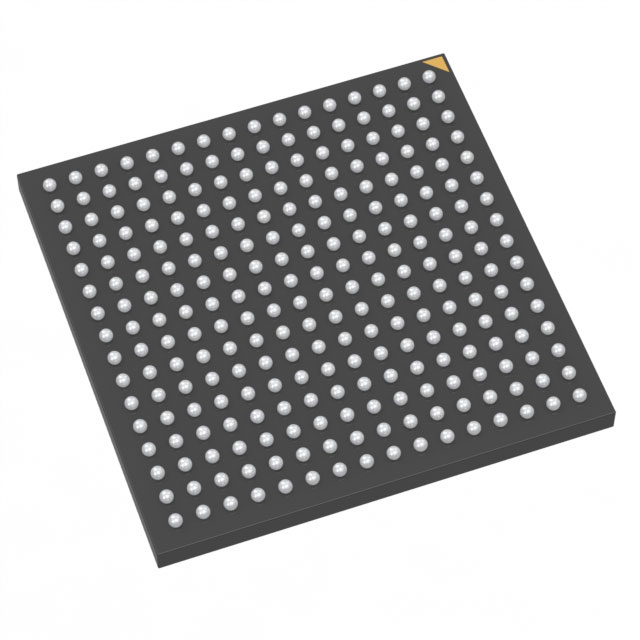
Axcelerator Field Programmable Gate Array (FPGA) IC 115 55296 208-BFCQFP with Tie Bar |
|---|---|
| Quantity | 340 Available (as of June 15, 2026) |

| Product Category | Field Programmable Gate Array (FPGA) |
|---|---|
| Manufacturer | Microchip Technology |
| Manufacturing Status | Active |
| Manufacturer Standard Lead Time | 44 Weeks |
| Datasheet |
Specifications & Environmental
| Device Package | 208-CQFP (75x75) | Grade | Military | Operating Temperature | -55°C – 125°C | ||
|---|---|---|---|---|---|---|---|
| Package / Case | 208-BFCQFP with Tie Bar | Number of I/O | 115 | Voltage | 1.425 V - 1.575 V | ||
| Mounting Method | Surface Mount | RoHS Compliance | RoHS non-compliant | REACH Compliance | REACH Unaffected | ||
| Moisture Sensitivity Level | 3 (168 Hours) | Number of LABs/CLBs | 4224 | Number of Logic Elements/Cells | 4224 | ||
| Number of Gates | 250000 | ECCN | 3A001A2C | HTS Code | 8542.39.0001 | ||
| Qualification | N/A | Total RAM Bits | 55296 |
Overview of AX250-CQ208M – Axcelerator Field Programmable Gate Array (FPGA) IC, 115 I/O, 55,296‑bit RAM, 208‑BFCQFP
The AX250-CQ208M is a military-grade Axcelerator antifuse FPGA offered in a 208‑BFCQFP package with tie bar. Based on Microchip's AX architecture, this device provides deterministic timing, on‑chip embedded SRAM/FIFO, and a high level of integration suited for mission‑critical and high‑reliability systems.
Designed for applications requiring robust operating range and security, the device combines 250,000 equivalent system gates, 4,224 logic elements, approximately 0.055 Mbits of embedded memory, and 115 user I/Os to support complex logic integration in a single, nonvolatile chip.
Key Features
- Core Capacity — 250,000 equivalent system gates with 4,224 logic elements, enabling substantial on‑chip logic integration for complex designs.
- Embedded Memory — Total RAM bits: 55,296 (approximately 0.055 Mbits) with embedded FIFO control logic for buffering and data‑stream management.
- I/O and Interfaces — 115 user I/Os provided in a banked, mixed‑voltage capable architecture as described by the Axcelerator family features.
- Performance — Family datasheet specifies 350+ MHz system performance and 500+ MHz internal performance, supporting high‑speed logic operation.
- Security and Programmability — Antifuse, single‑chip nonvolatile architecture with FuseLock programming technology to protect against reverse engineering and design theft.
- Clocking and Timing — Segmentable clock resources and embedded PLLs with frequency synthesis capabilities noted in the Axcelerator family documentation.
- Package and Mounting — Surface mount 208‑BFCQFP with tie bar (supplier package listed as 208‑CQFP, 75×75 mm footprint) for PCB assembly.
- Power and Voltage — Core supply 1.425 V to 1.575 V to match system power rails.
- Operating Range — Military grade with an operating temperature range of −55 °C to 125 °C for harsh‑environment deployment.
- Standards and Testability — Family includes boundary‑scan testing compliant with IEEE 1149.1 (JTAG) for board‑level manufacturing test and diagnostics.
- RoHS Compliance — Device is RoHS‑compliant.
Typical Applications
- Defense and Aerospace Systems — Military‑grade temperature range and nonvolatile antifuse architecture make the AX250‑CQ208M suitable for avionics, tactical radios, and mission‑critical control electronics.
- Secure Infrastructure — FuseLock programming and antifuse nonvolatility provide a hardware foundation for secure, tamper‑resistant logic in communications and security appliances.
- High‑Reliability Embedded Control — On‑chip RAM/FIFO and deterministic timing are useful for real‑time data buffering and control tasks in industrial and ruggedized equipment.
- High‑Performance DSP/Logic Integration — High internal performance and embedded FIFOs support data‑intensive logic functions and custom signal‑processing pipelines.
Unique Advantages
- Nonvolatile Antifuse Architecture: Eliminates the need for external configuration memory and provides a single‑chip, permanently programmed solution for reliable field operation.
- Military Temperature Qualification: Rated from −55 °C to 125 °C to meet stringent environmental requirements for defense and aerospace deployments.
- Integrated Memory and FIFO Logic: Approximately 55,296 bits of embedded RAM with programmable FIFO control logic reduces external memory requirements and simplifies board design.
- Security Features: FuseLock programming technology guards intellectual property and reduces risk of reverse engineering.
- High Logic Density: 250,000 equivalent system gates and 4,224 logic elements allow significant on‑chip integration, lowering BOM count and board complexity.
- Production Testability: IEEE 1149.1 (JTAG) boundary‑scan support facilitates board testing and debugging during manufacturing.
Why Choose AX250-CQ208M?
The AX250‑CQ208M positions itself as a high‑density, secure, and rugged FPGA option within the Axcelerator family, combining substantial logic capacity with embedded RAM and FIFO capabilities. Its antifuse nonvolatile nature and FuseLock protection make it an appropriate choice where long‑term reliability and IP security are priorities.
This device is a strong fit for engineers and procurement teams developing military, aerospace, and other high‑reliability systems who need deterministic timing, on‑chip memory, and a wide operating temperature range, all delivered in a 208‑pin CQFP surface‑mount package.
Request a quote or submit a sales inquiry to obtain pricing, lead times, and availability for the AX250‑CQ208M. Our team can provide detailed ordering information and support for integrating this Axcelerator FPGA into your design.


Date Founded: 1989
Headquarters: Chandler, Arizona, USA
Employees: 22,000+
Revenue: $8.349 Billion
Certifications and Memberships: ISO9001:2015, IATF16949:2016, AS 9100D


