
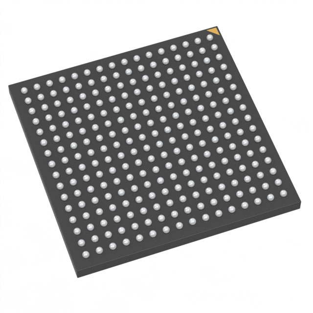
AX250-FG256I
| Part Description |
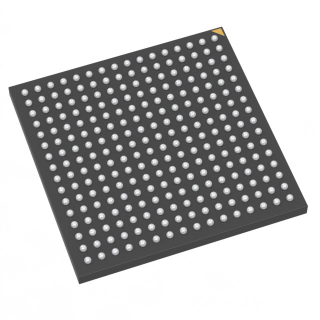
Axcelerator Field Programmable Gate Array (FPGA) IC 138 55296 256-LBGA |
|---|---|
| Quantity | 402 Available (as of October 8, 2026) |
| Product Category | Field Programmable Gate Array (FPGA) |
|---|---|
| Manufacturer | Microchip Technology |
| Manufacturing Status | Active |
| Manufacturer Standard Lead Time | 8 Weeks |
| Datasheet |
Specifications & Environmental
| Device Package | 256-FPBGA (17x17) | Grade | Industrial | Operating Temperature | -40°C – 85°C | ||
|---|---|---|---|---|---|---|---|
| Package / Case | 256-LBGA | Number of I/O | 138 | Voltage | 1.425 V - 1.575 V | ||
| Mounting Method | Surface Mount | RoHS Compliance | RoHS non-compliant | REACH Compliance | REACH Unaffected | ||
| Moisture Sensitivity Level | 3 (168 Hours) | Number of LABs/CLBs | 4224 | Number of Logic Elements/Cells | 4224 | ||
| Number of Gates | 250000 | ECCN | 3A991D | HTS Code | 8542.39.0001 | ||
| Qualification | N/A | Total RAM Bits | 55296 |
Overview of AX250-FG256I – Axcelerator Field Programmable Gate Array (FPGA) IC 138 55296 256-LBGA
The AX250-FG256I is a Microchip Axcelerator antifuse FPGA based on the AX architecture, offering a single‑chip, nonvolatile programmable logic solution. This industrial‑grade device provides 250,000 equivalent system gates and is built for designs that require secure, high‑performance programmable logic with integrated memory, PLLs and flexible I/O.
Designed on a 0.15 μm CMOS antifuse process with seven metal layers, the device supports deterministic timing and in‑system diagnostic capabilities while operating over an industrial temperature range and a 1.425–1.575 V core supply.
Key Features
- Logic Capacity — 250,000 equivalent system gates and 4,224 logic elements (cells) to implement complex logic and control functions.
- Embedded Memory & FIFOs — 55,296 bits of embedded RAM (approximately 0.055 Mbits) with embedded FIFO control logic for buffering and data staging inside the FPGA.
- I/O Resources — 138 user I/Os with multi‑standard I/O capability (mixed voltages supported at the family level) and LVDS‑capable interfaces up to 700 Mb/s.
- Performance — Family‑level performance metrics include 350+ MHz system performance and 500+ MHz internal performance; the family also provides high‑performance embedded FIFOs and PLL frequency synthesis.
- Programmability & Security — Antifuse, single‑chip nonvolatile programming and FuseLock programming technology to protect against reverse engineering and design theft.
- Clocking & Timing — Segmentable clock resources and on‑chip PLLs with frequency synthesis capability; deterministic, user‑controllable timing for predictable system behavior.
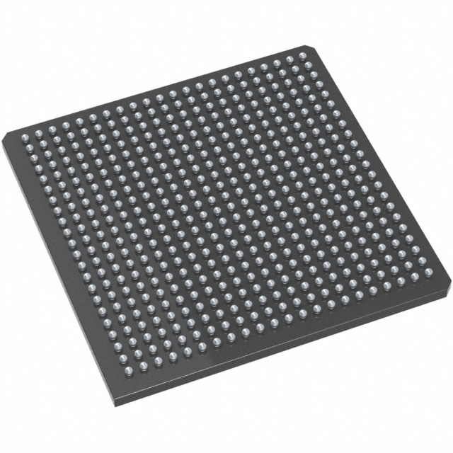
- Package & Mounting — 256‑LBGA package (supplier package: 256‑FPBGA, 17 × 17) for surface‑mount assembly; compact footprint compatible packaging.
- Industrial Grade & Environmental — Rated for operation from −40 °C to 85 °C and RoHS compliant.
- Power — Core supply range of 1.425 V to 1.575 V (nominal 1.5 V core voltage referenced at the family level) for low‑voltage operation.
Typical Applications
- High‑performance embedded systems — Use the device to accelerate compute‑intensive control or data‑path functions with dense logic and embedded memory.
- Secure, nonvolatile programmable logic — Antifuse programming and FuseLock protect IP in applications where design security and one‑time programmable configurations are required.
- I/O‑intensive interfaces — Leverage 138 I/Os and LVDS‑capable channels to implement mixed‑voltage interface bridging, serial links and high‑speed connectivity.
- Industrial control and instrumentation — Industrial temperature rating and deterministic timing make the device suitable for control, data acquisition and deterministic signal processing tasks.
Unique Advantages
- Nonvolatile, secure configuration: Antifuse technology and FuseLock programming provide a one‑time programmable, tamper‑resistant configuration for IP protection.
- Embedded RAM and FIFO support: On‑chip memory with configurable FIFO control simplifies buffer management and reduces external memory dependencies.
- Deterministic timing and clock flexibility: Segmentable clocks and on‑chip PLLs enable predictable timing and flexible clocking topologies for tightly constrained designs.
- Compact surface‑mount packaging: 256‑LBGA (256‑FPBGA supplier package) delivers a compact footprint for space‑constrained boards while maintaining ample I/O.
- Industrial operating range: −40 °C to 85 °C operation ensures suitability for a wide range of industrial environments.
- Vendor diagnostic support: In‑system diagnostic and debug capability is provided at the family level for streamlined bring‑up and validation.
Why Choose AX250-FG256I?
The AX250‑FG256I positions itself as a secure, high‑performance FPGA option within the Axcelerator family, combining 250,000 gates, 4,224 logic elements and embedded memory with antifuse nonvolatile programmability. Its mix of I/O density, embedded FIFOs, PLLs and deterministic timing make it well suited for industrial and high‑performance embedded designs that require long‑term configuration retention and design security.
Choosing this device provides a balance of integration, proven antifuse-based security and vendor diagnostic features that help reduce system BOM, simplify board-level design and support reliable operation across industrial temperature ranges.
Request a quote or submit an RFQ to confirm pricing, availability and lead time for the AX250‑FG256I. Our team can provide technical details and support to help you evaluate the device for your design."





















Date Founded: 1989
Headquarters: Chandler, Arizona, USA
Employees: 22,000+
Revenue: $8.349 Billion
Certifications and Memberships: ISO9001:2015, IATF16949:2016, AS 9100D




