
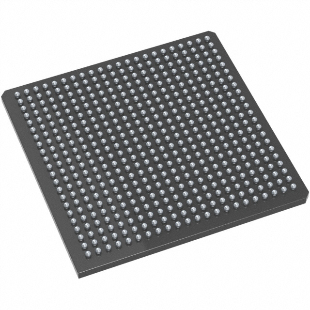
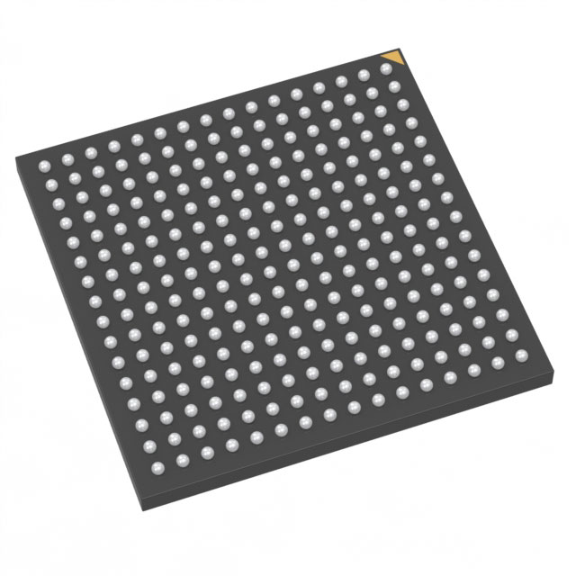
AX250-FG484
| Part Description |
Axcelerator Field Programmable Gate Array (FPGA) IC 248 55296 484-BGA |
|---|---|
| Quantity | 1,633 Available (as of June 15, 2026) |
| Product Category | Field Programmable Gate Array (FPGA) |
|---|---|
| Manufacturer | Microchip Technology |
| Manufacturing Status | Active |
| Manufacturer Standard Lead Time | 8 Weeks |
| Datasheet |
Specifications & Environmental
| Device Package | 484-FPBGA (23x23) | Grade | Commercial | Operating Temperature | 0°C – 70°C | ||
|---|---|---|---|---|---|---|---|
| Package / Case | 484-BGA | Number of I/O | 248 | Voltage | 1.425 V - 1.575 V | ||
| Mounting Method | Surface Mount | RoHS Compliance | RoHS non-compliant | REACH Compliance | REACH Unaffected | ||
| Moisture Sensitivity Level | 3 (168 Hours) | Number of LABs/CLBs | 4224 | Number of Logic Elements/Cells | 4224 | ||
| Number of Gates | 250000 | ECCN | 3A991D | HTS Code | 8542.39.0001 | ||
| Qualification | N/A | Total RAM Bits | 55296 |
Overview of AX250-FG484 – Axcelerator Field Programmable Gate Array (FPGA) IC 248 55296 484-BGA
The AX250-FG484 is a commercial-grade Axcelerator antifuse FPGA from Microchip Technology based on the AX architecture. It delivers a mid-range programmable logic solution with 250,000 equivalent system gates, segmentable clocking, embedded SRAM/FIFO control logic and on-chip PLL capability.
Designed for applications that need deterministic timing, secure nonvolatile configuration and flexible mixed-voltage I/O, the device combines performance-oriented silicon with embedded memory and high-speed I/O capability in a 484-ball FPBGA package.
Key Features
- Core & Logic 250,000 equivalent system gates and 4,224 logic elements provide mid-range capacity for complex glue logic, protocol handling and state-machine implementations.
- Embedded Memory & FIFOs 55,296 bits of on-chip SRAM with programmable embedded FIFO control logic enable buffering and width-configurable read/write ports for streaming and packetized data handling.
- I/O Flexibility 248 user I/Os with bank-selectable mixed-voltage operation (1.5V, 1.8V, 2.5V, 3.3V). Supports single-ended standards (LVTTL, LVCMOS, 3.3V PCI/PCI‑X) and differential standards including LVDS and LVPECL; LVDS I/Os are capable of 700 Mb/s operation.
- Clocking & PLL Segmentable clock resources and embedded PLLs with a 14–200 MHz input range and frequency synthesis capability up to 1 GHz for flexible clock management and clock-domain crossing strategies.
- Deterministic Timing & Debug Deterministic, user-controllable timing supported by in-system diagnostic and debug capability (Microchip Silicon Explorer II) for predictable timing closure and post-program debugging.
- Nonvolatile, Secure Programming Antifuse, single-chip nonvolatile solution manufactured on a 0.15 μm CMOS antifuse process with FuseLock programming technology to protect against reverse engineering and design theft.
- Power & Package Core supply range 1.425 V to 1.575 V (nominal 1.5 V) and commercial operating temperature 0 °C to 70 °C. Supplied in a 484-FPBGA (23 × 23) / 484-BGA package for surface-mount board integration.
- Standards & Compliance RoHS-compliant manufacturing and footprint-compatible packaging options for consistent assembly and regulatory compliance.
Typical Applications
- High-speed serial links LVDS-capable I/Os (700 Mb/s) and programmable PLLs enable implementation of high-speed differential interfaces and data link endpoints.
- Streaming and buffering On-chip SRAM and embedded FIFO control logic provide local buffering for data streaming, packet buffering or interface width conversion.
- Mixed-voltage integration Bank-selectable mixed-voltage I/Os support bridging and protocol translation between 1.5V, 1.8V, 2.5V and 3.3V domains on a single device.
- Secure, nonvolatile logic Antifuse, single-chip nonvolatile configuration and FuseLock technology make the device suitable for designs that require a secure, permanently programmed logic element.
Unique Advantages
- Highly integrated mid-range capacity: 250,000 equivalent system gates with 4,224 logic elements and 248 I/Os reduce external glue logic and simplify board-level design.
- On-chip memory with FIFO control: 55,296 bits of embedded SRAM and programmable FIFO logic enable efficient local data handling without external RAM.
- Flexible, multi-standard I/Os: Bank-selectable I/O voltages and broad support for single-ended and differential standards ease integration across multiple interface types.
- Secure, nonvolatile programming: Antifuse architecture combined with FuseLock safeguards IP and eliminates the need for external configuration memory.
- Deterministic timing and debug: User-controllable timing and in-system diagnostic capability support predictable performance and streamlined debugging.
- Commercial-grade, board-ready package: 484-FPBGA (23 × 23) surface-mount package and RoHS compliance facilitate volume assembly for commercial applications.
Why Choose AX250-FG484?
The AX250-FG484 occupies a capability sweet spot for mid-range FPGA designs that require a balance of logic capacity, on-chip memory and flexible, high-speed I/O. Its antifuse, single-chip nonvolatile architecture and FuseLock programming provide a secure, permanent configuration option while embedded PLLs and deterministic timing support performance-sensitive designs.
Choose this device if your design demands a commercial-grade FPGA with 250k gates, extensive mixed-voltage I/O, integrated SRAM/FIFO control and board-ready 484-FPBGA packaging—backed by Microchip’s Axcelerator architecture and the diagnostic features documented in the product datasheet.
Request a quote or submit an inquiry to receive pricing, lead-time and availability information for AX250-FG484.


Date Founded: 1989
Headquarters: Chandler, Arizona, USA
Employees: 22,000+
Revenue: $8.349 Billion
Certifications and Memberships: ISO9001:2015, IATF16949:2016, AS 9100D


