
AX250-FGG256
| Part Description |
Axcelerator Field Programmable Gate Array (FPGA) IC 138 55296 256-LBGA |
|---|---|
| Quantity | 639 Available (as of June 18, 2026) |

| Product Category | Field Programmable Gate Array (FPGA) |
|---|---|
| Manufacturer | Microchip Technology |
| Manufacturing Status | Active |
| Manufacturer Standard Lead Time | 8 Weeks |
| Datasheet |
Specifications & Environmental
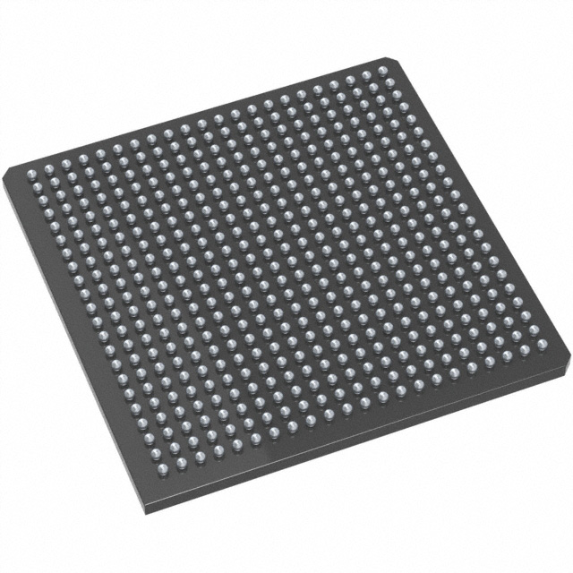
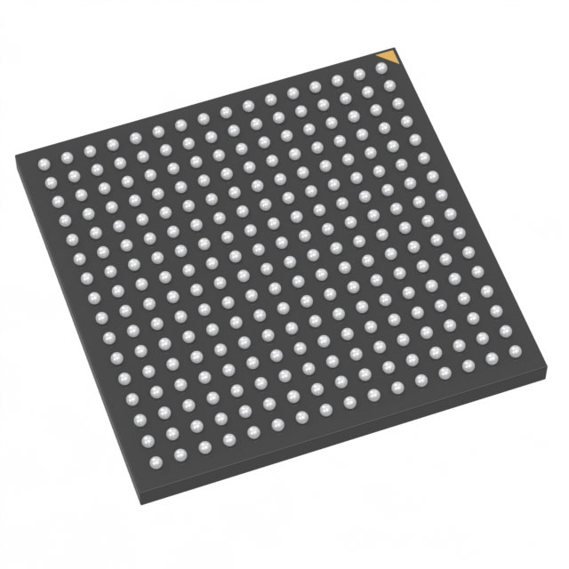
| Device Package | 256-FPBGA (17x17) | Grade | Commercial | Operating Temperature | 0°C – 70°C | ||
|---|---|---|---|---|---|---|---|
| Package / Case | 256-LBGA | Number of I/O | 138 | Voltage | 1.425 V - 1.575 V | ||
| Mounting Method | Surface Mount | RoHS Compliance | ROHS3 Compliant | REACH Compliance | REACH Unaffected | ||
| Moisture Sensitivity Level | 3 (168 Hours) | Number of LABs/CLBs | 4224 | Number of Logic Elements/Cells | 4224 | ||
| Number of Gates | 250000 | ECCN | 3A991D | HTS Code | 8542.39.0001 | ||
| Qualification | N/A | Total RAM Bits | 55296 |
Overview of AX250-FGG256 – Axcelerator FPGA, 250,000 Equivalent System Gates, 256-LBGA
The AX250-FGG256 is an Axcelerator field programmable gate array (FPGA) IC from Microchip Technology. It is an antifuse-based, single-chip nonvolatile FPGA built on the AX architecture and designed to deliver deterministic timing, design security and high internal performance.
Targeted at designs that require on-chip embedded memory, flexible multi-standard I/Os and high internal clock rates, this commercial-grade device provides secure, nonvolatile programmability with package and power characteristics suited for surface-mount applications.
Key Features
- Core capacity and logic elements – Approximately 250,000 equivalent system gates with 4,224 logic elements.
- Embedded memory – 55,296 bits of on-chip RAM (approximately 0.055 Mbits) with support for variable-aspect 4,608-bit RAM blocks and programmable embedded FIFO control logic.
- I/O and multi-standard interface support – 138 user I/Os; family-level support for mixed-voltage bank operation (1.5V, 1.8V, 2.5V, 3.3V) and differential standards including LVDS with 700 Mb/s capability.
- High-performance timing – Family-level published performance includes 350+ MHz system performance and 500+ MHz internal performance, segmentable clock resources and embedded PLLs with frequency synthesis capabilities.
- Security and diagnostics – FuseLock programming technology to protect against reverse engineering and built-in in-system diagnostic and debug capability referenced in the Axcelerator family documentation.
- Package, power and mounting – 256-LBGA package (supplier device package 256-FPBGA, 17×17), surface-mount mounting, and a core voltage supply range of 1.425 V to 1.575 V.
- Commercial operating range and compliance – Commercial grade with an operating temperature of 0 °C to 70 °C and RoHS compliance.
Typical Applications
- High-speed protocol bridging – Use the device’s high internal performance and LVDS-capable I/Os for protocol conversion and high-speed interface implementation.
- Embedded FIFO and buffering – Leverage on-chip RAM and embedded FIFO control logic for packet buffering, stream alignment and data rate matching.
- Custom logic and system glue – Implement application-specific datapaths, control logic and timing-critical modules where deterministic timing is required.
- Secure, nonvolatile designs – Apply FuseLock programming technology for designs that require on-chip nonvolatile programmability and protection against reverse engineering.
Unique Advantages
- Nonvolatile single-chip solution: Antifuse-based Axcelerator architecture provides one-time programmable, nonvolatile logic in a single component, simplifying design for secure applications.
- High internal performance: Documented family-level internal and system performance numbers support timing-critical logic and high-throughput data paths.
- Flexible I/O standards: Mixed-voltage bank operation and multi-standard support reduce external level-shifting and simplify board-level interfacing.
- On-chip memory and FIFO support: Embedded RAM and programmable FIFO control logic enable local buffering and width-conversion without external memory.
- Design protection: FuseLock programming technology and in-system diagnostic features enhance IP protection and aid bring-up and debug.
Why Choose AX250-FGG256?
AX250-FGG256 combines a substantial logic capacity (approximately 250k equivalent gates) with embedded memory, flexible I/O and antifuse nonvolatile programmability to address designs that demand secure, deterministic FPGA behavior. Its family-level performance characteristics and embedded PLLs make it suitable where internal timing and high-speed interfacing matter.
This commercial-grade device is a practical choice for engineers building communication interfaces, embedded buffering systems and custom logic implementations that benefit from a single-chip, protected FPGA solution with surface-mount 256-LBGA packaging and RoHS compliance.
Request a quote or submit an RFQ to check availability, pricing and lead times for the AX250-FGG256.


Date Founded: 1989
Headquarters: Chandler, Arizona, USA
Employees: 22,000+
Revenue: $8.349 Billion
Certifications and Memberships: ISO9001:2015, IATF16949:2016, AS 9100D


