
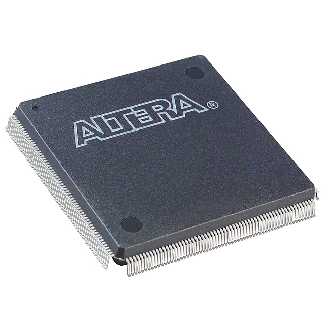
EP1C6Q240C7
| Part Description |
Cyclone® Field Programmable Gate Array (FPGA) IC 185 92160 5980 240-BFQFP |
|---|---|
| Quantity | 1,330 Available (as of June 15, 2026) |
| Product Category | Field Programmable Gate Array (FPGA) |
|---|---|
| Manufacturer | Intel |
| Manufacturing Status | Obsolete |
| Manufacturer Standard Lead Time | Contact Us |
| Datasheet |
Specifications & Environmental
| Device Package | 240-PQFP (32x32) | Grade | Commercial | Operating Temperature | 0°C – 85°C | ||
|---|---|---|---|---|---|---|---|
| Package / Case | 240-BFQFP | Number of I/O | 185 | Voltage | 1.425 V - 1.575 V | ||
| Mounting Method | Surface Mount | RoHS Compliance | RoHS non-compliant | REACH Compliance | REACH Unknown | ||
| Moisture Sensitivity Level | 3 (168 Hours) | Number of LABs/CLBs | 598 | Number of Logic Elements/Cells | 5980 | ||
| Number of Gates | N/A | ECCN | 3A991D | HTS Code | 8542.39.0001 | ||
| Qualification | N/A | Total RAM Bits | 92160 |
Overview of EP1C6Q240C7 – Cyclone® Field Programmable Gate Array (FPGA) IC 185 92160 5980 240-BFQFP
The EP1C6Q240C7 is a Cyclone® family FPGA offering a balanced combination of logic, embedded memory and I/O for commercial embedded and data-path applications. It is based on the Cyclone architecture described in the device handbook and is implemented on a 1.5‑V, 0.13‑µm, all-layer copper SRAM process.
With 5,980 logic elements, approximately 92 Kbits of embedded memory and 185 user I/O pins in a 240‑pin PQFP form factor, this device is targeted at designers requiring mid-range programmable logic for interface bridging, memory control and general-purpose digital processing within a commercial temperature range.
Key Features
- Logic Capacity — 5,980 logic elements provide mid-range programmable logic resources for control, glue-logic and data-path functions.
- Embedded Memory — Approximately 92 Kbits of on-chip RAM suitable for small buffering, FIFOs and state storage.
- I/O and Interfaces — 185 user I/O pins enable broad connectivity; the Cyclone family supports multiple I/O standards and high-speed LVDS signalling as described in the device handbook.
- Clocking Resources — Device-level support for up to two PLLs for clock multiplication and phase adjustment as documented for the Cyclone family.
- Package and Mounting — 240‑pin BFQFP package (supplier device package listed as 240‑PQFP, 32×32) in a surface-mount package for PCB integration.
- Power — Core supply operating range of 1.425 V to 1.575 V consistent with the Cyclone device family process requirements.
- Commercial Grade — Rated for 0 °C to 85 °C operation and specified as commercial grade.
- Standards and Configuration — Cyclone devices support common memory interfaces (including DDR SDRAM) and peripheral standards such as 66‑ and 33‑MHz PCI in the family documentation; configuration options include low-cost serial configuration devices.
- RoHS Compliant — Device is compliant with RoHS environmental requirements.
Typical Applications
- Data-Path Processing — Mid-range logic and on-chip RAM suited for packet processing, signal routing and data-path control functions.
- Memory Interface Bridging — Used to implement DDR SDRAM and SDRAM interface logic and buffering as supported by the Cyclone family.
- High-Speed I/O and Protocol Bridging — Ideal for implementing LVDS links, PCI-compatible peripheral interfaces or other multi-standard I/O bridging tasks.
- Embedded Control and Prototyping — Provides reconfigurable logic for control paths, user interfaces and development platforms within a commercial temperature environment.
Unique Advantages
- Balanced Integration: Combines nearly 6,000 logic elements with embedded RAM and extensive I/O to reduce external component count and simplify board design.
- Flexible I/O Support: Family-level support for multiple I/O standards and high-speed LVDS enables broad interface compatibility and system-level flexibility.
- On-Die Clocking: Up to two PLLs provide clock multiplication and phase shifting to simplify clock-domain management without additional ICs.
- Standard Package for Easy Assembly: 240-pin QFP/PQFP surface-mount package fits common PCB assembly flows and supports migration across Cyclone densities in similar packages.
- Environmentally Compliant: RoHS compliance helps meet regulatory requirements for commercial electronic products.
Why Choose EP1C6Q240C7?
The EP1C6Q240C7 positions itself as a practical, mid-density Cyclone FPGA option for designers who need a mix of logic resources, embedded memory and broad I/O in a commercial-grade, surface-mount package. Its combination of approximately 5,980 logic elements, roughly 92 Kbits of on-chip RAM, 185 I/O pins and family-level support for common memory and interface standards makes it well suited to interface bridging, data-path control and embedded system prototyping.
For product designs that prioritize predictable supply voltage requirements (1.425–1.575 V), available PLL-based clocking and a 240‑pin PQFP footprint, the EP1C6Q240C7 offers a reliable, standards-aligned option backed by the Cyclone device documentation and ecosystem.
Request a quote or submit an inquiry to receive pricing, availability and volume purchase options for the EP1C6Q240C7.


Date Founded: 1968
Headquarters: Santa Clara, California, USA
Employees: 130,000+
Revenue: $54.23 Billion
Certifications and Memberships: ISO9001:2015, ISO14001:2015, ISO17025:2017, ISO27001:2022, ISO45001:2018, ISO50001:2018


