
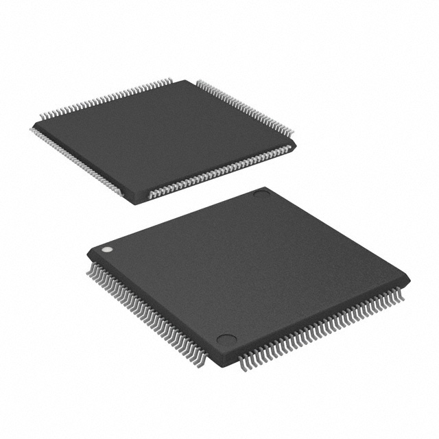
EP1C6T144C7
| Part Description |
Cyclone® Field Programmable Gate Array (FPGA) IC 98 92160 5980 144-LQFP |
|---|---|
| Quantity | 955 Available (as of June 15, 2026) |

| Product Category | Field Programmable Gate Array (FPGA) |
|---|---|
| Manufacturer | Intel |
| Manufacturing Status | Obsolete |
| Manufacturer Standard Lead Time | Contact Us |
| Datasheet |
Specifications & Environmental
| Device Package | 144-TQFP (20x20) | Grade | Commercial | Operating Temperature | 0°C – 85°C | ||
|---|---|---|---|---|---|---|---|
| Package / Case | 144-LQFP | Number of I/O | 98 | Voltage | 1.425 V - 1.575 V | ||
| Mounting Method | Surface Mount | RoHS Compliance | RoHS non-compliant | REACH Compliance | REACH Unknown | ||
| Moisture Sensitivity Level | 3 (168 Hours) | Number of LABs/CLBs | 598 | Number of Logic Elements/Cells | 5980 | ||
| Number of Gates | N/A | ECCN | 3A991D | HTS Code | 8542.39.0001 | ||
| Qualification | N/A | Total RAM Bits | 92160 |
Overview of EP1C6T144C7 – Cyclone® Field Programmable Gate Array (FPGA) IC, 98 I/O, ~92 Kbit RAM, 5,980 LEs, 144‑LQFP
The EP1C6T144C7 is a Cyclone® family FPGA in a 144‑pin LQFP/TQFP package designed for commercial-grade embedded and data-path applications. Built on the Cyclone architecture, this device combines 5,980 logic elements with on-chip embedded memory and dedicated clock resources to implement custom logic, peripheral interfaces, and memory controllers.
This surface-mount FPGA delivers a compact, low-voltage programmable solution with 98 user I/O pins and a supply voltage range of 1.425 V to 1.575 V, making it suitable for space-constrained PCBs that require moderate logic density and flexible I/O options.
Key Features
- Core Density — 5,980 logic elements (LEs) for implementing combinational and sequential logic, state machines, and glue logic in a single device.
- On-chip Memory — 92,160 total RAM bits, providing approximately 0.092 Mbits of embedded memory for FIFOs, buffers, and small data stores.
- I/O and Interface Support — 98 user I/O pins in the 144‑pin package. The Cyclone family supports multiple I/O standards including LVTTL, LVCMOS, SSTL‑2, SSTL‑3 and LVDS for flexible interfacing.
- Clocking — Two phase-locked loops (PLLs) available for clock multiplication and phase shifting to support differentiated clock domains and timing requirements.
- Configuration — Supports configuration through low-cost serial configuration devices as described for the Cyclone family.
- Power — Narrow core supply window of 1.425 V to 1.575 V for consistent power delivery and predictable DC operating conditions.
- Package & Mounting — 144‑LQFP package (supplier device package: 144‑TQFP, 20×20) in a surface-mount form factor for compact board-level integration.
- Commercial Grade & Environmental — Commercial temperature rating (0 °C to 85 °C) and RoHS‑compliant status.
Typical Applications
- Data-path logic and glue — Implement custom data processing pipelines, peripheral logic, and protocol bridging using the device’s 5,980 logic elements and embedded RAM.
- Memory interface controllers — Use built-in clocking and Cyclone family support for external memories (including DDR SDRAM in the family) when implementing memory controller logic and timing adjustments.
- High-speed serial/parallel I/O — Leverage the device’s variety of supported I/O standards and 98 user pins to interface sensors, SERDES endpoints, or peripherals requiring LVDS or LVCMOS signaling.
- Prototype and evaluation designs — A compact 144‑pin package and moderate logic density make the EP1C6T144C7 useful for development boards, proof-of-concept systems, and feature validation.
Unique Advantages
- Balanced logic and memory capacity — 5,980 LEs paired with approximately 92 Kbits of embedded RAM enable mixed logic and buffering tasks without external memory in many use cases.
- Flexible clocking — Two PLLs allow localized clock generation and phase adjustments to meet multi-domain timing requirements.
- Compact, surface-mount package — 144‑pin LQFP/TQFP footprint provides a dense pinout and easy PCB assembly for space-constrained systems.
- Low-voltage operation — A defined core supply range (1.425 V–1.575 V) supports predictable power design and supply sequencing on embedded platforms.
- Toolchain and migration support — Cyclone family documentation and Quartus® II support referenced for pin migration and device mapping across Cyclone densities, aiding design scalability.
- Regulatory and assembly readiness — RoHS compliance simplifies environmental compliance for commercial products.
Why Choose EP1C6T144C7?
The EP1C6T144C7 positions itself as a compact, commercially graded Cyclone FPGA option for designers needing moderate logic density, embedded memory, and flexible I/O in a 144‑pin surface-mount package. Its combination of 5,980 logic elements, approximately 92 Kbits of on-chip RAM, two PLLs, and support for industry I/O standards makes it well suited to data-path logic, interface bridging, and prototype systems.
Choose this device when you require a cost-effective, programmable component that integrates logic, memory, and clocking resources in a small footprint, and when you prefer a solution supported by Cyclone family documentation and the Quartus II design flow for migration and pin management.
Request a quote or submit a sales inquiry to obtain pricing, availability, and lead-time information for the EP1C6T144C7.


Date Founded: 1968
Headquarters: Santa Clara, California, USA
Employees: 130,000+
Revenue: $54.23 Billion
Certifications and Memberships: ISO9001:2015, ISO14001:2015, ISO17025:2017, ISO27001:2022, ISO45001:2018, ISO50001:2018


