
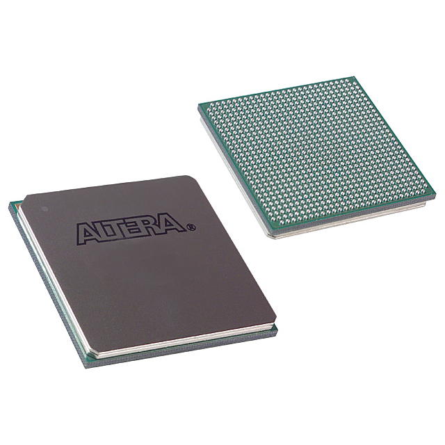
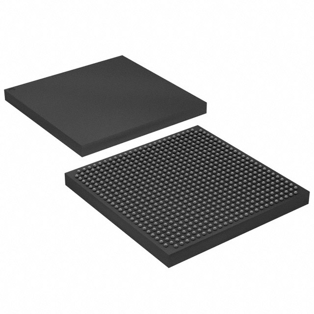
EP1S10F672C7
| Part Description |
Stratix® Field Programmable Gate Array (FPGA) IC 345 920448 10570 672-BBGA |
|---|---|
| Quantity | 1,520 Available (as of June 10, 2026) |

| Product Category | Field Programmable Gate Array (FPGA) |
|---|---|
| Manufacturer | Intel |
| Manufacturing Status | Obsolete |
| Manufacturer Standard Lead Time | Contact Us |
| Datasheet |
Specifications & Environmental
| Device Package | 672-FBGA (27x27) | Grade | Commercial | Operating Temperature | 0°C – 85°C | ||
|---|---|---|---|---|---|---|---|
| Package / Case | 672-BBGA | Number of I/O | 345 | Voltage | 1.425 V - 1.575 V | ||
| Mounting Method | Surface Mount | RoHS Compliance | RoHS non-compliant | REACH Compliance | REACH Unaffected | ||
| Moisture Sensitivity Level | 3 (168 Hours) | Number of LABs/CLBs | 1057 | Number of Logic Elements/Cells | 10570 | ||
| Number of Gates | N/A | ECCN | 3A991D | HTS Code | 8542.39.0001 | ||
| Qualification | N/A | Total RAM Bits | 920448 |
Overview of EP1S10F672C7 – Stratix® Field Programmable Gate Array, 672‑BBGA
The EP1S10F672C7 is a Stratix® family field programmable gate array (FPGA) IC from Intel, supplied in a 672‑BBGA (672‑FBGA, 27×27) surface‑mount package. It delivers a mid‑range balance of programmable logic, embedded memory, and high I/O count for complex board‑level digital designs.
Designed for applications that require programmable logic, on‑chip RAM, and flexible I/O and clocking options, this commercial‑grade device targets FPGA‑based designs where integration, configurability, and debug capability are important.
Key Features
- Core logic capacity — 10,570 logic elements and 1,057 LABs provide a mid‑range programmable fabric for glue logic, state machines, and custom datapaths.
- Embedded memory — Approximately 0.92 Mbits (920,448 bits) of on‑chip RAM supporting the Stratix TriMatrix memory architecture and multiple memory modes described in the device handbook.
- I/O resources — 345 dedicated I/O pins; Stratix I/O structure includes support for double‑data‑rate interfaces and advanced I/O standards as described in the device documentation.
- Clocking and PLLs — Stratix clocking architecture with PLL and clock network support, including enhanced and fast PLL options for flexible clock management.
- DSP & multiplier support — Device family documentation details multiplier and DSP block interfaces for implementing arithmetic and signal‑processing functions.
- Configuration and debug — Family features include IEEE 1149.1 (JTAG) boundary‑scan support, SignalTap II embedded logic analyzer capability, and multiple configuration modes and update options.
- Power and supply — Core supply voltage range of 1.425 V to 1.575 V, with power consumption and operating conditions specified in the Stratix device handbook.
- Package and mounting — 672‑BBGA / 672‑FBGA (27×27) surface‑mount package suitable for board‑level integration.
- Operating grade — Commercial grade with an operating temperature range of 0 °C to 85 °C.
- Standards and family documentation — Comprehensive Stratix device handbook coverage for architecture, I/O timing, PLLs, memory modes, and DC/switching characteristics to guide design and validation.
Typical Applications
- High‑density digital logic — Implement glue logic, control state machines, and custom finite‑state designs using the device's 10,570 logic elements and abundant I/O.
- Custom signal processing — Leverage on‑chip multipliers/DSP interfaces and embedded RAM for custom filtering, data formatting, and intermediate buffering.
- Board‑level I/O aggregation — Consolidate multiple interfaces and protocol conversions using 345 I/Os and Stratix I/O features including DDR support.
- Prototyping and development — Use JTAG boundary‑scan and the SignalTap II embedded logic analyzer for in‑system debug and iterative design refinement.
Unique Advantages
- Balanced logic and memory density: 10,570 logic elements paired with approximately 0.92 Mbits of embedded RAM enables a broad range of mid‑complexity designs without excessive external memory.
- High I/O availability: 345 I/Os reduce the need for external multiplexing or interface chips when aggregating signals and peripherals.
- Flexible clocking: Stratix PLLs and clock network options described in the device handbook provide multiple clocking modes for synchronous and high‑performance designs.
- Integrated debug and configuration options: JTAG boundary‑scan and SignalTap II support simplify bring‑up, testing, and in‑field configuration management.
- Board‑ready package: 672‑FBGA (27×27) surface‑mount package supports compact board designs and standardized assembly flows.
- Commercial operating range: Rated for 0 °C to 85 °C operation, suitable for a wide variety of commercial electronics applications.
Why Choose EP1S10F672C7?
The EP1S10F672C7 offers a pragmatic combination of programmable logic, embedded memory, and extensive I/O in a single Stratix family FPGA package. Its documented architecture, clocking options, and on‑chip resources make it a suitable choice for designers building mid‑complexity FPGA solutions that require in‑system debug, flexible configuration, and a standardized board‑level package.
Backed by the Stratix device handbook and Intel's device documentation, this part is appropriate for teams seeking a commercially graded FPGA with clear hardware capabilities and well‑documented design guidance.
Request a quote or submit an inquiry for pricing and availability to evaluate EP1S10F672C7 for your next FPGA design.


Date Founded: 1968
Headquarters: Santa Clara, California, USA
Employees: 130,000+
Revenue: $54.23 Billion
Certifications and Memberships: ISO9001:2015, ISO14001:2015, ISO17025:2017, ISO27001:2022, ISO45001:2018, ISO50001:2018


