
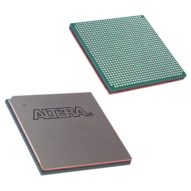
EP1SGX40DF1020C5N
| Part Description |
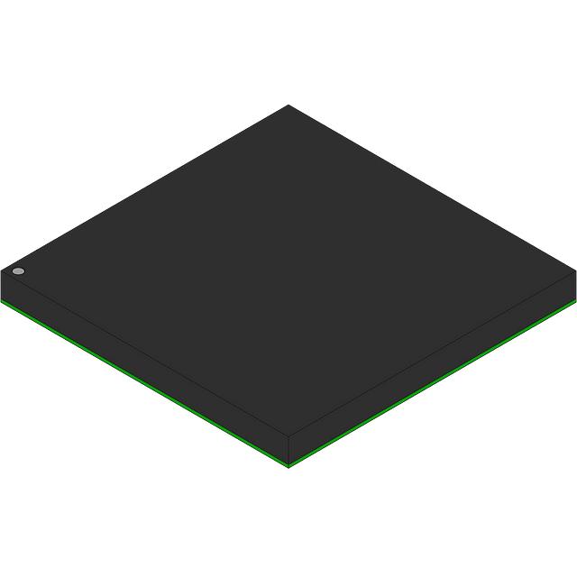
Stratix® GX Field Programmable Gate Array (FPGA) IC 624 3423744 41250 1020-BBGA |
|---|---|
| Quantity | 952 Available (as of October 7, 2026) |
| Product Category | Field Programmable Gate Array (FPGA) |
|---|---|
| Manufacturer | Intel |
| Manufacturing Status | Obsolete |
| Manufacturer Standard Lead Time | Contact Us |
| Datasheet |
Specifications & Environmental
| Device Package | 1020-FBGA (33x33) | Grade | Commercial | Operating Temperature | 0°C – 85°C | ||
|---|---|---|---|---|---|---|---|
| Package / Case | 1020-BBGA | Number of I/O | 624 | Voltage | 1.425 V - 1.575 V | ||
| Mounting Method | Surface Mount | RoHS Compliance | Unknown | REACH Compliance | REACH Unknown | ||
| Moisture Sensitivity Level | 3 (168 Hours) | Number of LABs/CLBs | 4125 | Number of Logic Elements/Cells | 41250 | ||
| Number of Gates | N/A | ECCN | 3A001A7A | HTS Code | 8542.39.0001 | ||
| Qualification | N/A | Total RAM Bits | 3423744 |
Overview of EP1SGX40DF1020C5N – Stratix® GX FPGA, 41,250 logic elements, 624 I/O, 1020-BBGA
The EP1SGX40DF1020C5N is a Stratix® GX family field programmable gate array (FPGA) IC offering a high-performance, scalable logic array combined with advanced high-speed serial transceiver capabilities. This commercial-grade, surface-mount device delivers 41,250 logic elements, approximately 3.4 Mbits of embedded RAM, and 624 I/O pins in a 1020-ball BGA footprint.
Designed for high-speed backplane interfaces, chip-to-chip links and communications protocol bridging, this device pairs a 1.5‑V logic architecture with configurable transceiver features and rich on-chip resources for systems that require integrated serial bandwidth and dense logic integration.
Key Features
- Core logic — 41,250 logic elements (LEs) implemented in a 1.5‑V logic array, delivering scalable logic density for complex FPGA designs.
- Embedded memory — Approximately 3.4 Mbits of on-chip RAM with TriMatrix™ memory architecture that supports multiple RAM block sizes for true dual-port memory and FIFO implementations.
- High-speed serial transceivers — Family-level support for full-duplex transceiver operation from 500 Mbps to 3.1875 Gbps with clock data recovery (CDR), programmable VOD, pre-emphasis and equalization, and individual channel power-down control.
- Protocol and SERDES support — Transceiver features and IP support for XAUI, Gigabit Ethernet, SONET/SDH and compatibility with PCI Express, SMPTE 292M, Fibre Channel and Serial RapidIO standards (as provided at the family level).
- I/O and interface flexibility — 624 device I/O pins with support for numerous single-ended and differential I/O standards, including LVDS, LVPECL and 3.3‑V PCML on reference clocks and receiver inputs; source-synchronous differential I/O for high-speed interfaces.
- DSP and performance blocks — Dedicated high-speed DSP blocks for multipliers and MAC/FIR implementations (specified faster than 300 MHz), enabling signal processing and arithmetic acceleration on-chip.
- Clocking and PLLs — Up to eight general-purpose PLLs per device region (four enhanced PLLs and four fast PLLs) offering spread-spectrum, programmable bandwidth, clock switchover and real-time reconfiguration.
- Package, power and thermal — 1020‑BBGA / 1020‑FBGA (33×33) package, surface-mount mounting type, supply voltage range 1.425 V to 1.575 V, and commercial operating temperature range 0 °C to 85 °C.
- Reliability and test — Built-in self-test (BIST), pattern detection/word alignment, 8B/10B encoding/decoding and hot insertion/removal protection circuitry available at the family feature level.
- RoHS compliant — Device is RoHS status compliant.
Typical Applications
- High-speed backplane interfaces — Use the integrated transceivers and dense logic to implement multi-gigabit backplane links and protocol bridging for networking equipment.
- Chip-to-chip communication — Leverage SERDES and CDR features for reliable, high-bandwidth chip-to-chip serial links in complex system boards.
- Communications protocol bridging — Implement protocol converters and aggregation functions using abundant logic, embedded memory and transceiver features.
- High-speed I/O subsystems — Build source-synchronous and differential I/O interfaces for packet processing, storage controllers or custom high-throughput peripherals.
Unique Advantages
- Integrated serial bandwidth and logic density: Combines multi-gigabit transceiver capabilities with 41,250 logic elements to consolidate functions that would otherwise require multiple chips.
- Significant embedded memory: Approximately 3.4 Mbits of on-chip RAM enables large buffers, FIFOs and data-path storage without external memory for many applications.
- Flexible transceiver tuning: Programmable VOD, pre-emphasis and equalization let designers optimize signal integrity for board-level and channel conditions.
- Dedicated DSP resources: High-speed DSP blocks (multipliers and MACs) accelerate signal processing tasks and offload compute from general logic.
- Comprehensive clock management: Multiple PLLs with real-time reconfiguration support complex clocking schemes and spread-spectrum requirements.
- Board-level integration ready: 1020‑BBGA package and surface-mount mounting make the device suitable for compact, high-density PCB designs.
Why Choose EP1SGX40DF1020C5N?
The EP1SGX40DF1020C5N positions itself as a high-performance, scalable FPGA solution when combined serial bandwidth and dense on-chip resources are required. With 41,250 logic elements, approximately 3.4 Mbits of embedded RAM, industry-oriented transceiver features and comprehensive clocking and DSP blocks, it suits designs that demand integrated serial I/O, protocol flexibility and significant on-chip processing.
This commercial-grade device is appropriate for engineering teams building high-speed communication subsystems, backplane interfaces, and chip-to-chip interconnects where a balance of logic density, embedded memory and configurable transceiver capability is essential. The package, supply voltage range and temperature rating support typical board-level deployment and system integration.
Request a quote or submit an inquiry to receive pricing and availability information for EP1SGX40DF1020C5N.
























Date Founded: 1968
Headquarters: Santa Clara, California, USA
Employees: 130,000+
Revenue: $54.23 Billion
Certifications and Memberships: ISO9001:2015, ISO14001:2015, ISO17025:2017, ISO27001:2022, ISO45001:2018, ISO50001:2018


