
EP20K100EBC356-3N
| Part Description |
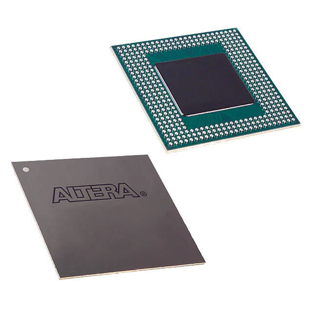
APEX-20KE® Field Programmable Gate Array (FPGA) IC 246 53248 4160 356-LBGA |
|---|---|
| Quantity | 632 Available (as of October 8, 2026) |

| Product Category | Field Programmable Gate Array (FPGA) |
|---|---|
| Manufacturer | Intel |
| Manufacturing Status | Obsolete |
| Manufacturer Standard Lead Time | Contact Us |
| Datasheet |
Specifications & Environmental
| Device Package | 356-BGA (35x35) | Grade | Commercial | Operating Temperature | 0°C – 85°C | ||
|---|---|---|---|---|---|---|---|
| Package / Case | 356-LBGA | Number of I/O | 246 | Voltage | 1.71 V - 1.89 V | ||
| Mounting Method | Surface Mount | RoHS Compliance | Unknown | REACH Compliance | REACH Unaffected | ||
| Moisture Sensitivity Level | 3 (168 Hours) | Number of LABs/CLBs | 416 | Number of Logic Elements/Cells | 4160 | ||
| Number of Gates | 263000 | ECCN | 3A001A2A | HTS Code | 8542.39.0001 | ||
| Qualification | N/A | Total RAM Bits | 53248 |
Overview of EP20K100EBC356-3N – APEX-20KE Field Programmable Gate Array (356‑LBGA)
The EP20K100EBC356-3N is an APEX-20KE family field programmable gate array (FPGA) manufactured by Intel. It implements a MultiCore architecture that integrates lookup-table (LUT) logic, product‑term logic and embedded system blocks (ESBs) to deliver flexible on‑chip logic and memory capabilities for commercial embedded designs.
With 4,160 logic elements, approximately 53,248 bits of embedded memory, and 246 user I/Os in a compact 356‑BGA (35×35) surface‑mount package, this device targets commercial applications requiring programmable logic, memory buffering and versatile I/O interfacing while supporting low‑power operation and advanced clock management.
Key Features
- Core architecture MultiCore architecture combining LUT logic, product‑term logic and embedded system blocks (ESBs) for register‑intensive and memory‑oriented functions.
- Logic capacity 4,160 logic elements and approximately 263,000 system gates provide mid‑range programmable logic capacity for custom datapaths and control logic.
- Embedded memory Approximately 0.053 Mbits (53,248 bits) of on‑chip RAM implemented in ESBs; ESBs can be used for FIFO buffers, dual‑port RAM and content‑addressable memory (CAM).
- I/O and signaling 246 user I/Os with MultiVolt I/O interface support enabling connectivity with 1.8 V, 2.5 V, 3.3 V and 5.0 V devices; family supports advanced I/O standards and high‑speed differential signaling such as LVDS.
- Clock management Family features include up to four phase‑locked loops (PLLs), up to eight global clocks and programmable clock features (ClockLock, ClockBoost, ClockShift) for flexible timing architectures.
- Power and supply Designed for low‑power operation; device supply range is 1.71 V to 1.89 V and ESBs include programmable power‑saving modes.
- Package and thermal 356‑LBGA (35×35) surface‑mount package; commercial grade with operating temperature range 0 °C to 85 °C. RoHS compliant.
Typical Applications
- PCI and expansion controllers Suited for PCI‑based board functions and bridging applications that require programmable I/O timing and bus interfacing.
- Memory interface and buffering Use ESBs to implement DDR/ZBT memory interfaces, FIFOs and dual‑port RAM for systems that need local buffering and memory arbitration.
- High‑speed serial and differential I/O Implement LVDS or other differential signaling channels for high‑throughput data paths and serializer/deserializer functions.
- Commercial embedded systems Ideal for custom control, protocol handling and glue‑logic in commercial‑grade embedded products requiring compact package and mid‑range logic density.
Unique Advantages
- Highly integrated solution: Combines 4,160 logic elements with ESB‑based embedded memory to reduce external component count and simplify board design.
- Flexible, voltage‑agnostic I/O: 246 user I/Os with MultiVolt support enable direct interfacing to a wide range of peripherals and legacy interfaces.
- Robust clocking and timing control: Multiple PLLs and programmable clock features let designers optimize clock domains and reduce skew across complex logic.
- Low‑power operation: Narrow internal supply range and ESB power‑saving modes support energy‑conscious designs in commercial applications.
- Compact BGA footprint: 356‑LBGA (35×35) surface‑mount package delivers a small board area for space‑constrained system designs.
Why Choose EP20K100EBC356-3N?
The EP20K100EBC356-3N offers a balanced combination of mid‑range logic density, embedded memory and flexible I/O in a compact 356‑BGA package. Its MultiCore architecture and ESB resources make it well suited for designs that require on‑chip buffering, custom logic implementation and multiple clock domains while operating within commercial temperature limits.
This device is appropriate for engineering teams building commercial embedded systems, board‑level expansion controllers, or memory interface logic who need a programmable, low‑power FPGA with proven family features and RoHS compliance.
Request a quote or submit a procurement inquiry to receive pricing and lead‑time information for the EP20K100EBC356-3N. Our team can provide technical and purchasing details to support your design and sourcing needs.























Date Founded: 1968
Headquarters: Santa Clara, California, USA
Employees: 130,000+
Revenue: $54.23 Billion
Certifications and Memberships: ISO9001:2015, ISO14001:2015, ISO17025:2017, ISO27001:2022, ISO45001:2018, ISO50001:2018


