
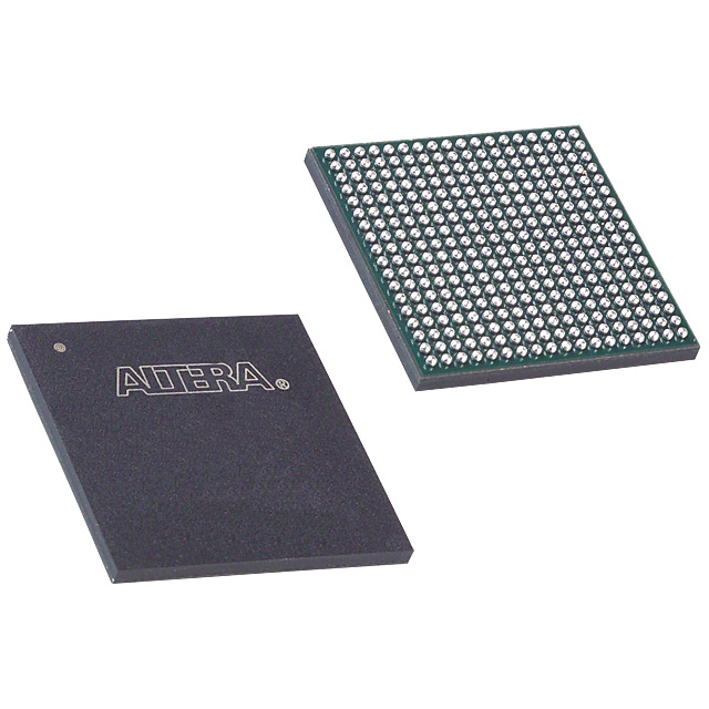
EP20K100EFC324-1
| Part Description |
APEX-20KE® Field Programmable Gate Array (FPGA) IC 246 53248 4160 324-BGA |
|---|---|
| Quantity | 104 Available (as of June 14, 2026) |

| Product Category | Field Programmable Gate Array (FPGA) |
|---|---|
| Manufacturer | Intel |
| Manufacturing Status | Obsolete |
| Manufacturer Standard Lead Time | Contact Us |
| Datasheet |
Specifications & Environmental
| Device Package | 324-FBGA (19x19) | Grade | Commercial | Operating Temperature | 0°C – 85°C | ||
|---|---|---|---|---|---|---|---|
| Package / Case | 324-BGA | Number of I/O | 246 | Voltage | 1.71 V - 1.89 V | ||
| Mounting Method | Surface Mount | RoHS Compliance | RoHS non-compliant | REACH Compliance | REACH Unaffected | ||
| Moisture Sensitivity Level | 3 (168 Hours) | Number of LABs/CLBs | 416 | Number of Logic Elements/Cells | 4160 | ||
| Number of Gates | 263000 | ECCN | 3A991D | HTS Code | 8542.39.0001 | ||
| Qualification | N/A | Total RAM Bits | 53248 |
Overview of EP20K100EFC324-1 – APEX-20KE® FPGA, 324‑BGA
The EP20K100EFC324-1 is an APEX-20KE family field programmable gate array (FPGA) from Intel, offered in a 324‑ball BGA (324‑FBGA, 19×19) surface-mount package. It combines a MultiCore architecture that integrates look-up table (LUT) logic, product-term logic and embedded system blocks (ESBs) to address logic-intensive and memory-intensive on‑chip functions.
With 4,160 logic elements, approximately 53,248 bits of embedded memory, and 246 user I/O pins, this device suits commercial designs requiring on‑chip FIFOs, dual-port RAM, CAM-style memory, flexible I/O and programmable clock management.
Key Features
- Core architecture MultiCore architecture integrating LUT logic, product-term logic and embedded system blocks (ESBs) for register‑ and combinatorial‑intensive functions.
- Logic capacity 4,160 logic elements and approximately 263,000 system gates, supporting complex combinational and sequential logic implementations.
- Embedded memory Approximately 53,248 bits of on‑chip RAM implemented via ESBs, usable for FIFOs, dual‑port RAM and CAM functions.
- I/O and interface flexibility 246 user I/O pins with MultiVolt I/O interface support and programmable I/O features for integration with a range of external devices and signaling levels.
- Clock management Built‑in clock resources including multiple PLLs, low‑skew clock tree and features for phase/shift and clock multiplication/division to support synchronized designs.
- Package and mounting 324‑BGA (324‑FBGA, 19×19) surface mount package suitable for compact board layouts.
- Power and supply Internal supply specified across 1.71 V to 1.89 V, enabling designs centered on the device’s 1.8 V core domain.
- Commercial operating range and compliance Commercial grade device rated for 0 °C to 85 °C operating temperature and RoHS compliant.
Typical Applications
- High‑performance embedded systems Use on‑chip ESBs and LUT logic to implement memory buffers, control logic and custom accelerators within commercial embedded platforms.
- Memory interface and buffering Implement DDR SDRAM or ZBT SRAM interface logic and FIFO buffering using the device’s embedded memory and I/O bandwidth.
- Peripheral and bus bridging Implement PCI/legacy bus bridging and custom peripheral controllers leveraging flexible I/O and programmable clocking.
- Data acquisition and interface logic Deploy LVDS or other high‑speed I/O signaling with programmable output control and dedicated clock resources for deterministic timing.
Unique Advantages
- Highly integrated architecture: MultiCore design with LUTs and ESBs reduces the need for external memory and discrete glue logic.
- Balanced logic and memory: 4,160 logic elements paired with approximately 53,248 bits of embedded RAM support mixed logic/memory functions on a single device.
- Flexible I/O strategy: 246 user I/Os and MultiVolt support enable interfaces across common system voltage domains without excessive external translation.
- Robust clocking features: On‑chip PLLs and low‑skew clock distribution simplify multi‑clock designs and timing closure.
- Compact packaging: 324‑FBGA (19×19) footprint allows high channel density in space‑constrained commercial boards.
- Regulatory and environmental readiness: RoHS compliance provides assurance for lead‑free manufacturing processes.
Why Choose EP20K100EFC324-1?
The EP20K100EFC324-1 positions itself as a commercially graded, mid‑density FPGA that combines a MultiCore logic architecture, dedicated embedded memory blocks and a comprehensive I/O feature set in a compact 324‑BGA package. Its combination of 4,160 logic elements, approximately 53 kb of embedded RAM and 246 I/Os makes it suitable for commercial applications that require on‑chip buffering, moderate logic density and flexible interfacing.
Designers seeking a platform with programmable clock management, adaptable I/O voltage support and on‑chip memory for FIFOs or dual‑port RAM will find this device appropriate for cost‑sensitive, performance‑oriented commercial systems where space and integration reduce BOM and board complexity.
Request a quote or submit an inquiry for pricing and availability to begin integrating the EP20K100EFC324-1 into your next commercial FPGA design.


Date Founded: 1968
Headquarters: Santa Clara, California, USA
Employees: 130,000+
Revenue: $54.23 Billion
Certifications and Memberships: ISO9001:2015, ISO14001:2015, ISO17025:2017, ISO27001:2022, ISO45001:2018, ISO50001:2018


