
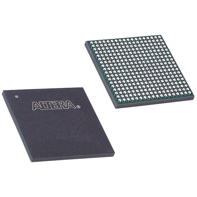
EP20K100EFC324-1N
| Part Description |
APEX-20KE® Field Programmable Gate Array (FPGA) IC 246 53248 4160 324-BGA |
|---|---|
| Quantity | 909 Available (as of June 14, 2026) |

| Product Category | Field Programmable Gate Array (FPGA) |
|---|---|
| Manufacturer | Intel |
| Manufacturing Status | Obsolete |
| Manufacturer Standard Lead Time | Contact Us |
| Datasheet |
Specifications & Environmental
| Device Package | 324-FBGA (19x19) | Grade | Commercial | Operating Temperature | 0°C – 85°C | ||
|---|---|---|---|---|---|---|---|
| Package / Case | 324-BGA | Number of I/O | 246 | Voltage | 1.71 V - 1.89 V | ||
| Mounting Method | Surface Mount | RoHS Compliance | Unknown | REACH Compliance | REACH Unaffected | ||
| Moisture Sensitivity Level | 3 (168 Hours) | Number of LABs/CLBs | 416 | Number of Logic Elements/Cells | 4160 | ||
| Number of Gates | 263000 | ECCN | 3A001A2A | HTS Code | 8542.39.0001 | ||
| Qualification | N/A | Total RAM Bits | 53248 |
Overview of EP20K100EFC324-1N – APEX-20KE FPGA, 324-BGA, 246 I/O
The EP20K100EFC324-1N is an APEX-20KE® field programmable gate array (FPGA) offered in a 324-ball BGA package (19×19). Built on the APEX 20K family architecture, it combines lookup-table (LUT) logic, product-term logic and embedded memory blocks (ESBs) to address register‑intensive, combinatorial and memory‑centric functions in commercial applications.
With 4,160 logic elements, approximately 53,248 bits of on‑chip RAM, 246 I/O pins and a rated internal supply window of 1.71 V to 1.89 V, this device targets mid-density programmable logic requirements where integration of logic, memory and flexible I/O is required within a compact surface‑mount package.
Key Features
- Core Architecture: MultiCore architecture integrating LUT logic and product‑term logic for a mix of register‑intensive and combinatorial functions.
- Logic Capacity: 4,160 logic elements and a maximum of 263,000 system gates provide mid‑density programmable logic suitable for complex control and glue‑logic tasks.
- Embedded Memory: Approximately 53,248 bits of embedded RAM (ESBs) to implement FIFOs, dual‑port RAM and content‑addressable memory functions.
- Macrocells: 416 macrocells available (device‑family figure) for product‑term based functions and legacy macrocell implementations.
- I/O and Packaging: 246 user I/O pins in a 324‑ball BGA (324‑FBGA, 19×19) surface‑mount package for compact board integration.
- Clock Management: Flexible clock resources with support for multiple PLLs and a built‑in low‑skew clock tree (family feature).
- Voltage and Power: Rated internal supply 1.71 V to 1.89 V; designed for low‑power operation with ESB‑based power‑saving modes (family feature).
- Operating Range and Grade: Commercial grade device with specified operating temperature of 0 °C to 85 °C.
- Standards and I/O Support: Family‑level support for multi‑voltage I/O interfaces and a wide range of I/O standards (as described in the device family datasheet).
Typical Applications
- Embedded Control and Glue Logic: Use the 4,160 logic elements and abundant I/O to implement control logic, protocol bridging and board‑level glue functions.
- Memory Interfaces and Buffers: Leverage approximately 53 Kbits of embedded RAM and ESB features to implement FIFOs, small buffers and dual‑port memory structures.
- High‑Performance I/O Connectivity: 246 I/O pins and family I/O features enable interfacing with external memories, buses and mixed‑voltage peripherals.
- Clocked System Functions: Built‑in clock management and PLL support facilitate clock distribution, multiplication/division and phase adjustments for synchronous designs.
Unique Advantages
- Balanced Integration: Combines LUT logic, product‑term logic and embedded memory in a single device to reduce component count and simplify board design.
- Mid‑Density Logic with On‑Chip RAM: 4,160 logic elements paired with ~53 Kbits of RAM enable compact implementations of control, buffering and small memory functions without external SRAM.
- Compact BGA Package: 324‑FBGA (19×19) surface‑mount package offers high I/O density in a compact footprint for space‑constrained PCBs.
- Flexible Clocking: Family features such as multiple PLLs and a low‑skew clock tree allow robust clock distribution for multi‑domain designs.
- Commercial Temperature Range: Specified 0 °C to 85 °C operation aligns with a broad range of commercial electronic applications.
Why Choose EP20K100EFC324-1N?
The EP20K100EFC324-1N delivers a balanced mid‑density FPGA solution combining 4,160 logic elements, embedded ESB memory and generous I/O in a compact 324‑ball BGA. It is well suited for designers who need a single‑chip programmable solution that integrates logic, memory and flexible clock/I/O capabilities for commercial applications.
Choosing this APEX‑20KE device provides continuity with the device family feature set—including ESB memory blocks, product‑term logic and flexible clock management—offering design scalability and predictable resource mapping for projects that require on‑chip memory and moderate logic capacity.
If you need pricing or availability, request a quote or submit an enquiry and our team will provide a prompt response with current lead time and ordering information.


Date Founded: 1968
Headquarters: Santa Clara, California, USA
Employees: 130,000+
Revenue: $54.23 Billion
Certifications and Memberships: ISO9001:2015, ISO14001:2015, ISO17025:2017, ISO27001:2022, ISO45001:2018, ISO50001:2018


