
EP20K100EFC324-2N
| Part Description |
APEX-20KE® Field Programmable Gate Array (FPGA) IC 246 53248 4160 324-BGA |
|---|---|
| Quantity | 704 Available (as of June 15, 2026) |

| Product Category | Field Programmable Gate Array (FPGA) |
|---|---|
| Manufacturer | Intel |
| Manufacturing Status | Obsolete |
| Manufacturer Standard Lead Time | Contact Us |
| Datasheet |
Specifications & Environmental
| Device Package | 324-FBGA (19x19) | Grade | Commercial | Operating Temperature | 0°C – 85°C | ||
|---|---|---|---|---|---|---|---|
| Package / Case | 324-BGA | Number of I/O | 246 | Voltage | 1.71 V - 1.89 V | ||
| Mounting Method | Surface Mount | RoHS Compliance | Unknown | REACH Compliance | REACH Unaffected | ||
| Moisture Sensitivity Level | 3 (168 Hours) | Number of LABs/CLBs | 416 | Number of Logic Elements/Cells | 4160 | ||
| Number of Gates | 263000 | ECCN | 3A991D | HTS Code | 8542.39.0001 | ||
| Qualification | N/A | Total RAM Bits | 53248 |
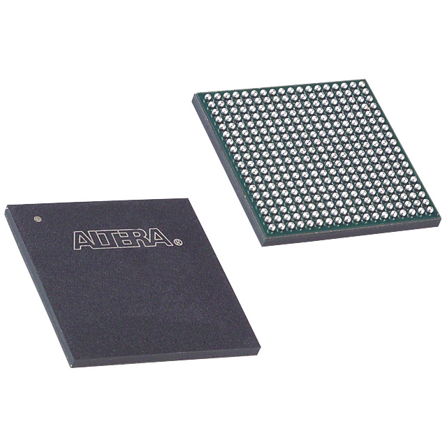
Overview of EP20K100EFC324-2N – APEX-20KE® FPGA, 4,160 logic elements, ~53,248-bit embedded memory, 246 I/O, 324-BGA
The EP20K100EFC324-2N is an APEX-20KE series Field Programmable Gate Array (FPGA) in a 324-ball BGA package, delivering 4,160 logic elements and approximately 53,248 bits of embedded RAM. It integrates MultiCore architecture components—look-up table (LUT) logic, product-term logic and embedded system blocks (ESBs)—for compact system implementation and flexible on-chip memory usage.
Designed for commercial applications, this device targets designs that require moderate logic density, abundant I/O (246 pins), multi-voltage I/O interfacing and flexible clock management while operating from a 1.71 V to 1.89 V core supply within a 0 °C to 85 °C temperature range.
Key Features
- MultiCore architecture Integrates LUT logic, product-term logic and embedded system blocks (ESBs) to implement register‑intensive and memory functions on-chip.
- Logic resources 4,160 logic elements providing implementation capacity equivalent to the device’s listed 263,000 gates for mid-range programmable logic designs.
- Embedded memory Approximately 53,248 bits of on‑chip RAM available for FIFOs, dual-port RAM and content-addressable memory (CAM) implementations via ESBs.
- Rich I/O 246 user I/O pins with MultiVolt I/O support for 1.8 V, 2.5 V, 3.3 V and 5.0 V interfaces and programmable output slew-rate and clamp options.
- Clock management Flexible clocking with up to four phase-locked loops (PLLs), built-in low-skew clock tree and features such as ClockBoost, ClockShift and ClockLock for phase/delay control.
- High-speed interfaces Support for high-speed external memories (including DDR SDRAM and ZBT SRAM) and LVDS performance up to 840 Mbits per channel; PCI 3.3 V compliance for 33/66 MHz operation is supported by the device family.
- Power and supply Core operating range specified at 1.71 V to 1.89 V and power-saving modes available via ESB configuration.
- Package & mounting 324‑ball FBGA (19 × 19 mm) surface-mount package suited for compact board-level integration.
- Commercial temperature grade Rated for 0 °C to 85 °C operation and RoHS compliant.
Typical Applications
- System-on-programmable-chip (SOPC) integration — Implement embedded controllers, custom peripherals and system glue logic using the device’s MultiCore architecture and ESBs.
- Memory interface controllers — Implement DDR SDRAM and ZBT SRAM interfaces using on-chip memory and high-speed I/O capability.
- PCI-based expansion and bridging — Support for PCI 3.3 V operation enables use in bus-interface and expansion card designs.
- High-speed serial and differential signaling — LVDS-capable channels (up to 840 Mbits/channel) suit high-throughput links and protocol conversion tasks.
Unique Advantages
- Highly integrated MultiCore design: Combines LUTs, product-term logic and ESBs to reduce external components and consolidate system functions on-chip.
- Balanced logic and memory resources: 4,160 logic elements paired with ~53 Kbits of embedded RAM enable mixed compute-and-buffer architectures without large external memory dependency.
- Flexible I/O and voltage compatibility: MultiVolt I/O and programmable clamps simplify interfacing to a wide range of legacy and modern peripherals.
- Robust clocking features: Up to four PLLs plus ClockBoost/ClockShift/ClockLock options allow designers to manage skew, multiply/divide clocks and fine-tune timing on complex designs.
- Compact BGA footprint: 324-FBGA (19 × 19 mm) package provides high I/O density in a space-efficient form factor for board-level integration.
- Standards-oriented I/O support: Family-level support for PCI, LVDS and common memory interfaces helps shorten design cycles for interface-intensive applications.
Why Choose EP20K100EFC324-2N?
The EP20K100EFC324-2N positions itself as a mid-density, feature-rich FPGA option within the APEX-20KE family, offering a practical balance of logic elements, embedded RAM and high I/O count in a compact 324‑BGA package. Its MultiCore architecture and ESB-based memory enable integration of both logic and buffering functions on-chip, reducing external BOM and simplifying system architecture.
This device is well suited for commercial designs that require multi-voltage I/O compatibility, flexible clock management and support for high-speed memory and serial interfaces. The combination of available resources, package density and family-level features makes it a fit for embedded systems, interface controllers and I/O-heavy FPGA implementations where board space and integration matter.
Request a quote or submit an inquiry for pricing and availability to evaluate the EP20K100EFC324-2N for your next design.


Date Founded: 1968
Headquarters: Santa Clara, California, USA
Employees: 130,000+
Revenue: $54.23 Billion
Certifications and Memberships: ISO9001:2015, ISO14001:2015, ISO17025:2017, ISO27001:2022, ISO45001:2018, ISO50001:2018


