
EP20K100EQC240-2X
| Part Description |
APEX-20KE® Field Programmable Gate Array (FPGA) IC 183 53248 4160 240-BFQFP |
|---|---|
| Quantity | 695 Available (as of June 16, 2026) |

| Product Category | Field Programmable Gate Array (FPGA) |
|---|---|
| Manufacturer | Intel |
| Manufacturing Status | Obsolete |
| Manufacturer Standard Lead Time | Contact Us |
| Datasheet |
Specifications & Environmental
| Device Package | 240-PQFP (32x32) | Grade | Commercial | Operating Temperature | 0°C – 85°C | ||
|---|---|---|---|---|---|---|---|
| Package / Case | 240-BFQFP | Number of I/O | 183 | Voltage | 1.71 V - 1.89 V | ||
| Mounting Method | Surface Mount | RoHS Compliance | RoHS non-compliant | REACH Compliance | REACH Unaffected | ||
| Moisture Sensitivity Level | 3 (168 Hours) | Number of LABs/CLBs | 416 | Number of Logic Elements/Cells | 4160 | ||
| Number of Gates | 263000 | ECCN | 3A991D | HTS Code | 8542.39.0001 | ||
| Qualification | N/A | Total RAM Bits | 53248 |
Overview of EP20K100EQC240-2X – APEX-20KE® FPGA, 4,160 logic elements, 53,248-bit RAM, 183 I/O
The EP20K100EQC240-2X is an APEX-20KE family field-programmable gate array (FPGA) IC designed for commercial embedded logic applications. It implements a MultiCore architecture that integrates look-up table (LUT) logic, product-term logic and embedded memory, enabling system-on-a-programmable-chip (SOPC) integration.
This device targets applications that require medium-density programmable logic combined with embedded system blocks, plentiful I/O and flexible clock management—delivering a balance of integration, configurability and power-aware operation for embedded and communications designs.
Key Features
- MultiCore architecture and SOPC integration Integrates LUT logic, product-term logic and embedded memory to support register‑intensive and memory‑intensive functions within a single programmable device.
- Logic density Approximately 263,000 gates with 4,160 logic elements, suitable for medium-density logic implementations and complex glue logic.
- Embedded memory Approximately 53,248 bits of on-chip RAM implemented in embedded system blocks (ESBs) for FIFOs, dual-port RAM and CAM-style functions.
- I/O capability 183 user I/O pins with MultiVolt I/O interface support to interface with multiple voltage domains and a programmable slew and clamp options for signal integrity control.
- Clock and timing Flexible clock management with up to four PLLs, built-in low-skew clock tree and multiple global clock signals to manage complex timing domains.
- Power and voltage Low-voltage internal operation with supply range specified at 1.71 V to 1.89 V and design considerations for low-power modes.
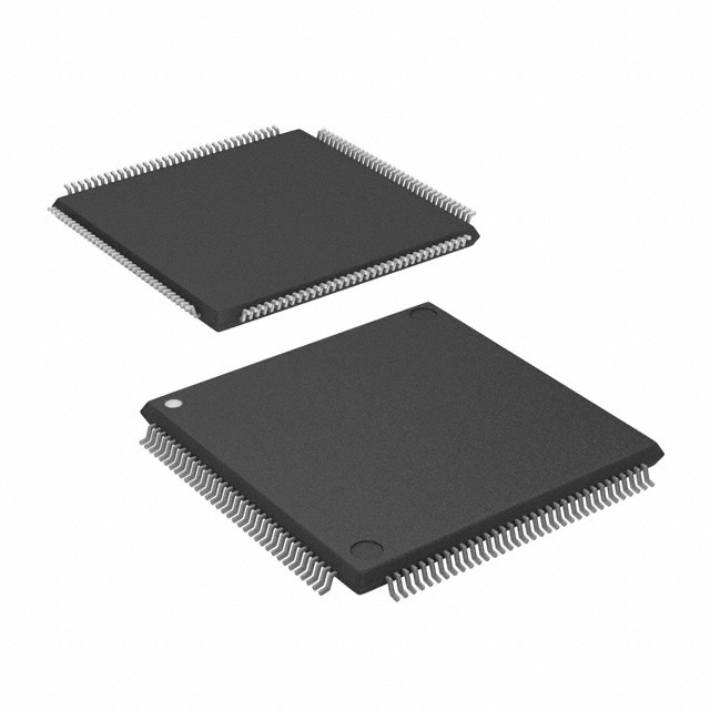
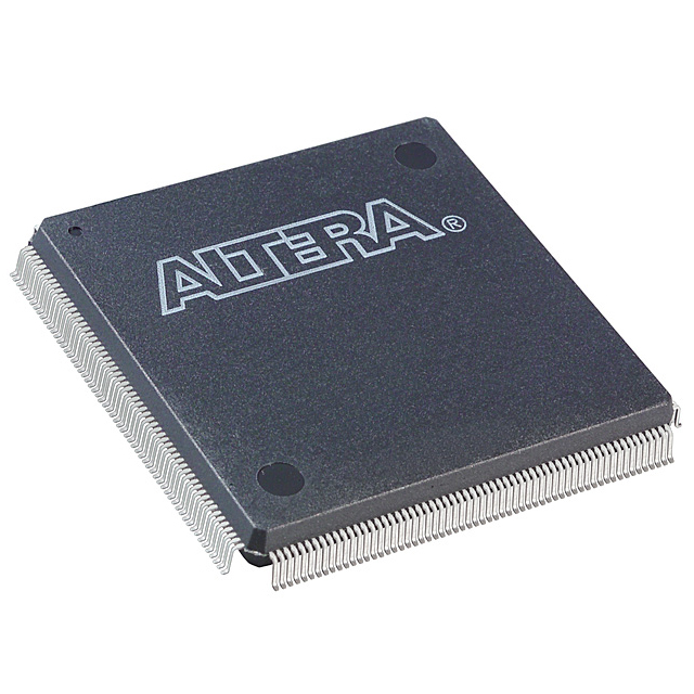
- Package and mounting 240-BFQFP (240-PQFP 32×32) surface-mount package for streamlined PCB assembly and compact board-level integration.
- Commercial temperature grade Rated for 0 °C to 85 °C operation and RoHS compliant for standard commercial deployments.
Typical Applications
- Embedded systems and SOPC solutions — Use on-chip LUTs and ESBs to consolidate control logic, FIFOs and custom peripherals in compact embedded designs.
- Interface bridging and protocol conversion — Leverage abundant I/O and MultiVolt support to interface between different voltage domains and legacy or modern peripherals.
- Memory buffering and data streaming — Implement FIFOs and dual-port RAM using the device’s embedded memory for buffering in data acquisition, buffering or communications paths.
- Prototyping and development — Medium-density logic and flexible clock resources make this FPGA suitable for breadboarding and early-stage hardware development of custom logic.
Unique Advantages
- Integrated SOPC-capable architecture: MultiCore integration of LUTs, product-term logic and ESBs reduces external component count and simplifies system design.
- Balanced logic and memory resources: 4,160 logic elements with approximately 53,248 bits of on-chip RAM provide a practical balance for designs that mix control logic and buffering.
- Flexible I/O for mixed-voltage systems: 183 user I/O pins and MultiVolt interface support simplify interconnection to peripherals across multiple voltage domains.
- Robust clock management: Multiple PLLs and a low-skew clock tree enable reliable multi‑domain timing without extensive external logic.
- Compact, surface-mount package: 240-BFQFP package supports dense board layouts while remaining compatible with standard PCB assembly processes.
- Commercial-grade, RoHS-compliant: Rated 0 °C to 85 °C and RoHS compliant for mainstream electronic products and systems.
Why Choose EP20K100EQC240-2X?
The EP20K100EQC240-2X positions itself as a flexible, medium-density FPGA offering a practical mix of logic, embedded memory and I/O resources in a compact surface-mount package. Its MultiCore SOPC-oriented architecture and on-chip ESBs make it well suited for designers who need to consolidate control logic, buffering and interface glue into a single programmable device.
This device is ideal for development teams and OEMs building commercial embedded systems, communications interfaces or prototype platforms that require predictable timing, mixed-voltage I/O support and a balance of logic and memory resources backed by the APEX-20KE device family feature set.
Request a quote or submit an inquiry to receive pricing, availability and technical support information for the EP20K100EQC240-2X.


Date Founded: 1968
Headquarters: Santa Clara, California, USA
Employees: 130,000+
Revenue: $54.23 Billion
Certifications and Memberships: ISO9001:2015, ISO14001:2015, ISO17025:2017, ISO27001:2022, ISO45001:2018, ISO50001:2018


