
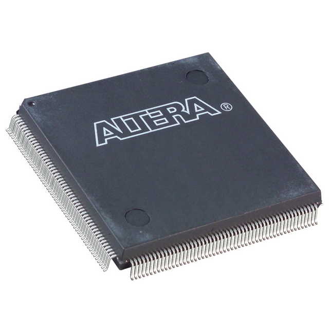
EP20K100EQC240-1N
| Part Description |
APEX-20KE® Field Programmable Gate Array (FPGA) IC 183 53248 4160 240-BFQFP |
|---|---|
| Quantity | 776 Available (as of June 10, 2026) |

| Product Category | Field Programmable Gate Array (FPGA) |
|---|---|
| Manufacturer | Intel |
| Manufacturing Status | Obsolete |
| Manufacturer Standard Lead Time | Contact Us |
| Datasheet |
Specifications & Environmental
| Device Package | 240-PQFP (32x32) | Grade | Commercial | Operating Temperature | 0°C – 85°C | ||
|---|---|---|---|---|---|---|---|
| Package / Case | 240-BFQFP | Number of I/O | 183 | Voltage | 1.71 V - 1.89 V | ||
| Mounting Method | Surface Mount | RoHS Compliance | Unknown | REACH Compliance | REACH Unaffected | ||
| Moisture Sensitivity Level | 3 (168 Hours) | Number of LABs/CLBs | 416 | Number of Logic Elements/Cells | 4160 | ||
| Number of Gates | 263000 | ECCN | 3A991D | HTS Code | 8542.39.0001 | ||
| Qualification | N/A | Total RAM Bits | 53248 |
Overview of EP20K100EQC240-1N – APEX-20KE FPGA, 4,160 logic elements, 53,248-bit embedded memory, 183 I/O (240‑BFQFP)
The EP20K100EQC240-1N is an APEX-20KE family field programmable gate array (FPGA) designed for system-level integration and mid-density logic implementations. It leverages the APEX 20K family architecture, including MultiCore integration and embedded system blocks (ESBs), to combine lookup-table logic, product-term logic, and on-chip RAM for memory and FIFO functions.
With 4,160 logic elements, approximately 53,248 bits of embedded RAM, and 183 user I/O pins in a 240‑pin BFQFP package, this commercial-grade device targets designs requiring moderate logic capacity, flexible I/O support, and on-chip memory for buffering and local storage.
Key Features
- Core & Architecture APEX 20K MultiCore architecture integrating LUT logic, product-term logic, and embedded system blocks (ESBs) for mixed register- and memory-oriented functions.
- Logic Capacity 4,160 logic elements (LEs) with a device gate count of 263,000, delivering mid-range programmable logic resources for control, glue logic, and moderate compute tasks.
- Embedded Memory Approximately 53,248 bits of on-chip RAM provided by ESBs that can implement FIFOs, dual-port RAM, and content-addressable memory (CAM) structures.
- I/O & Interfaces 183 user I/O pins with family-level support for MultiVolt I/O standards and advanced interfaces; suitable for high-speed external memories and differential signaling applications.
- Clocking & Timing Family clock management features include up to four PLLs, a built-in low-skew clock tree, and support for multiple global clocks and programmable clock phase/delay controls.
- Power & Voltage Device supply specified at 1.71 V to 1.89 V. Family features include low-power design elements and ESB programmable power-saving modes.
- Package & Mounting 240-BFQFP (240‑PQFP, 32×32) surface-mount package for PCB assembly where a compact PQFP footprint is required.
- Operating Conditions Commercial grade with an operating temperature range of 0 °C to 85 °C and RoHS compliance for environmental requirements.
Typical Applications
- System integration and SOPC designs Use the MultiCore architecture and ESBs to implement embedded system functions, on-chip peripherals, and custom logic in system-on-programmable-chip applications.
- Memory interface controllers On-chip RAM and ESB capabilities support FIFO buffers and controllers for DDR SDRAM and other external memory interfaces.
- High-speed I/O bridging Broad I/O pin count and family support for high-speed standards enable PCI/PCI-X-like bus bridging, LVDS links, and protocol conversion tasks.
- Prototyping and mid-density designs Moderate logic and embedded memory make this device suitable for prototyping feature sets and deploying production designs that require up to a few thousand LEs and dedicated on-chip RAM.
Unique Advantages
- Integrated MultiCore architecture Combines LUT, product-term logic, and ESBs to simplify mapping of register-intensive and memory-intensive functions within one device.
- On-chip RAM for buffering and CAM Approximately 53,248 bits of embedded memory enable local data storage, FIFOs, and CAM implementations without external memory.
- Flexible clock management Multiple PLLs and programmable clock features support complex timing domains and reduce clock skew across the design.
- High I/O count in a compact package 183 user I/O pins in a 240‑BFQFP package provide extensive interfacing capability while maintaining a small board footprint.
- Commercial temperature and RoHS compliance Operational range of 0 °C to 85 °C and RoHS compliance support standard commercial product requirements and environmental regulations.
Why Choose EP20K100EQC240-1N?
The EP20K100EQC240-1N offers a balanced mix of programmable logic, embedded memory, and flexible I/O suitable for mid-density FPGA applications. It is well matched to designs that need roughly 4,160 logic elements, on-chip RAM for buffering and local storage, and a high pin count in a 240‑pin PQFP footprint.
For engineers and procurement teams building system-level integrations, protocol bridges, or memory interface controllers in commercial-temperature environments, this APEX-20KE device delivers a consistent, verifiable feature set with the packaging and supply characteristics needed for production deployment.
If you would like pricing, availability, or a formal quote for EP20K100EQC240-1N, submit a quote request or contact procurement to receive a prompt response.


Date Founded: 1968
Headquarters: Santa Clara, California, USA
Employees: 130,000+
Revenue: $54.23 Billion
Certifications and Memberships: ISO9001:2015, ISO14001:2015, ISO17025:2017, ISO27001:2022, ISO45001:2018, ISO50001:2018


