
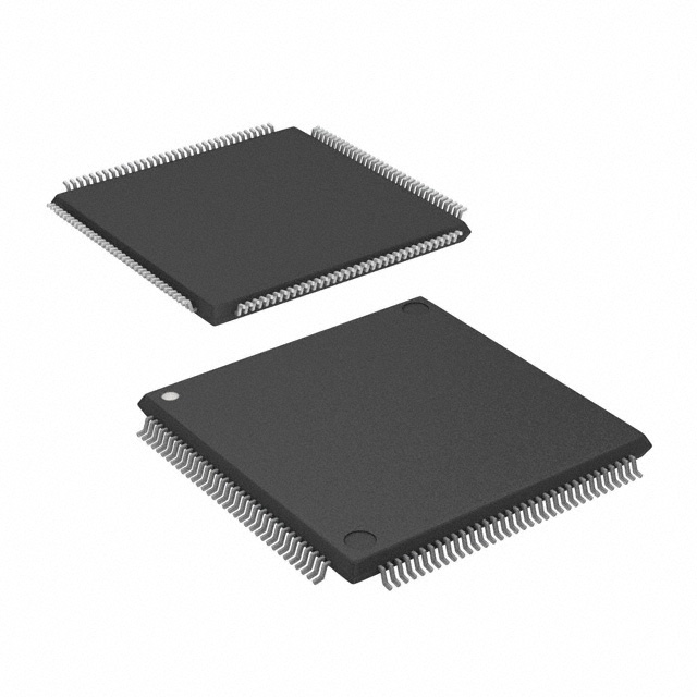
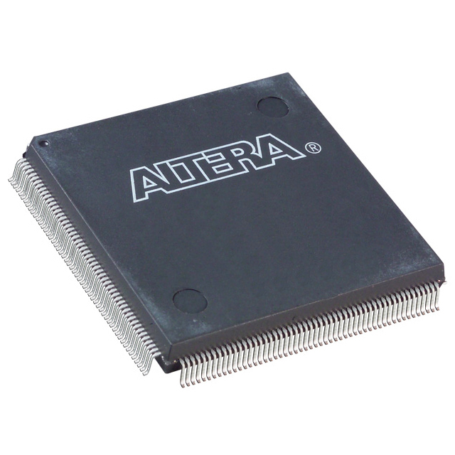
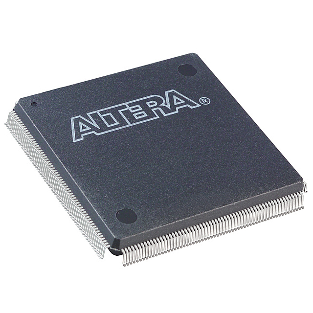
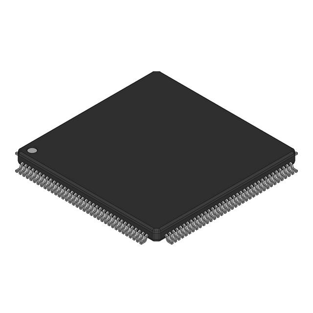
EP20K100TC144-1
| Part Description |
APEX-20K® Field Programmable Gate Array (FPGA) IC 101 53248 4160 144-LQFP |
|---|---|
| Quantity | 1,587 Available (as of June 18, 2026) |
| Product Category | Field Programmable Gate Array (FPGA) |
|---|---|
| Manufacturer | Intel |
| Manufacturing Status | Obsolete |
| Manufacturer Standard Lead Time | Contact Us |
| Datasheet |
Specifications & Environmental
| Device Package | 144-TQFP (20x20) | Grade | Commercial | Operating Temperature | 0°C – 85°C | ||
|---|---|---|---|---|---|---|---|
| Package / Case | 144-LQFP | Number of I/O | 101 | Voltage | 2.375 V - 2.625 V | ||
| Mounting Method | Surface Mount | RoHS Compliance | Unknown | REACH Compliance | REACH Unaffected | ||
| Moisture Sensitivity Level | 3 (168 Hours) | Number of LABs/CLBs | 416 | Number of Logic Elements/Cells | 4160 | ||
| Number of Gates | 263000 | ECCN | 3A001A2A | HTS Code | 8542.39.0001 | ||
| Qualification | N/A | Total RAM Bits | 53248 |
Overview of EP20K100TC144-1 – APEX-20K® Field Programmable Gate Array (FPGA) IC 101 53248 4160 144-LQFP
The EP20K100TC144-1 is an Intel APEX-20K® family FPGA offered in a 144-LQFP package. It implements the APEX MultiCore architecture with lookup-table (LUT) logic, product-term logic and embedded system blocks (ESBs) to support on-chip memory and combinatorial functions.
Designed for commercial-grade applications, this device provides a balanced combination of logic capacity, embedded memory and flexible I/O for system integration, memory interfaces and embedded control tasks.
Key Features
- Core architecture MultiCore architecture with LUT logic, product-term logic and embedded system blocks (ESBs) for implementing register-intensive and memory functions.
- Logic capacity 4,160 logic elements and a system-gates capability reported at 263,000, enabling mid-range programmable logic designs.
- Embedded memory Total on-chip RAM: 53,248 bits (approximately 53 kbits) available through ESBs for FIFOs, dual-port RAM and CAM-style implementations.
- I/O and interface support 101 user I/O pins with MultiVolt I/O interface concepts described in the family datasheet, plus support in the family for high-speed memory interfaces and LVDS and PCI-related signaling options.
- Clock management Family-level features include flexible clock circuitry with multiple PLLs, a low-skew clock tree, and programmable clock phase/delay options for deterministic timing.
- Power and supply Device internal supply range listed as 2.375 V to 2.625 V; family supports low-power operation and MultiVolt I/O interface options.
- Packaging and temperature Surface-mount 144-LQFP package (supplier device package noted as 144-TQFP, 20×20) and commercial temperature grade with specified operating range 0 °C to 85 °C.
- Standards and compliance RoHS compliant per supplier declaration.
Typical Applications
- Embedded system integration Use on designs that require on-chip memory and combinatorial logic integration for control and data-path functions.
- Memory interface and buffering ESB-based RAM and FIFO implementations support designs that need local buffering or dual-port memory structures for external memory subsystems.
- High-speed I/O and protocol bridging Suitable where flexible I/O signaling and programmable logic are needed to implement bus adapters, protocol bridges or custom I/O timing.
- Prototyping and mid-range FPGA functions Provides a mid-level logic resource set for development platforms and feature-rich prototypes that require integrated LUT and ESB resources.
Unique Advantages
- Integrated MultiCore architecture: Combines LUT logic and ESBs to implement both register-intensive and memory-centric functions on a single device.
- Balanced logic and memory resources: 4,160 logic elements and approximately 53 kbits of embedded RAM provide a good balance for control and data buffering tasks without external parts.
- Flexible clocking: Family-level clock management capabilities (multiple PLLs, low-skew clock tree, programmable phase/delay) help manage complex timing domains.
- Commercial-grade reliability: Specified for 0 °C to 85 °C operation and supplied in a compact 144-LQFP surface-mount package for standard commercial applications.
- RoHS compliant: Conforms to RoHS requirements, supporting environmentally conscious product designs.
Why Choose EP20K100TC144-1?
The EP20K100TC144-1 brings APEX-20K family architecture into a compact, commercial-grade 144-LQFP package—delivering 4,160 logic elements, over 53 kbits of embedded RAM and flexible I/O pin count for mid-range programmable-logic designs. Its MultiCore approach and ESB resources make it suitable for designs that require on-chip memory, combinatorial logic and flexible clock management.
This device is well suited for customers building embedded controllers, interface adapters and prototyping platforms that benefit from on-chip memory and integrated logic. The combination of verified APEX family features and commercial-grade packaging supports scalable deployments where vendor ecosystem and documented device capabilities matter.
If you would like pricing, availability or a formal quote for EP20K100TC144-1, submit a request for a quote or product inquiry to receive details on lead time and ordering options.


Date Founded: 1968
Headquarters: Santa Clara, California, USA
Employees: 130,000+
Revenue: $54.23 Billion
Certifications and Memberships: ISO9001:2015, ISO14001:2015, ISO17025:2017, ISO27001:2022, ISO45001:2018, ISO50001:2018


