
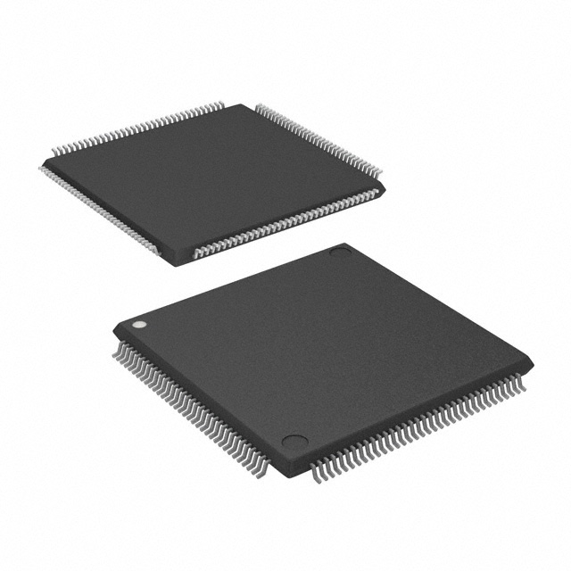
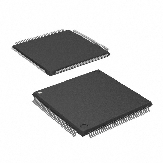
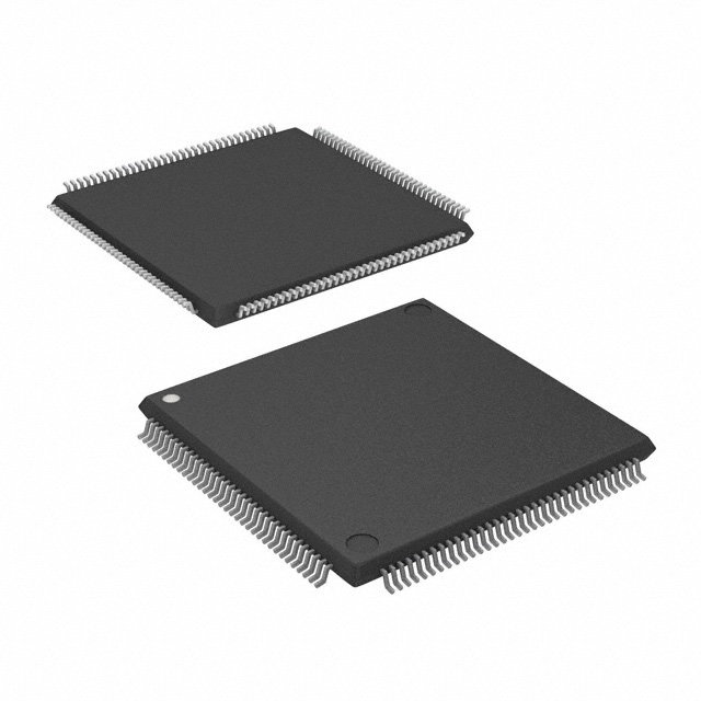
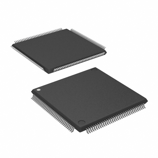
EP20K100TC144-3
| Part Description |
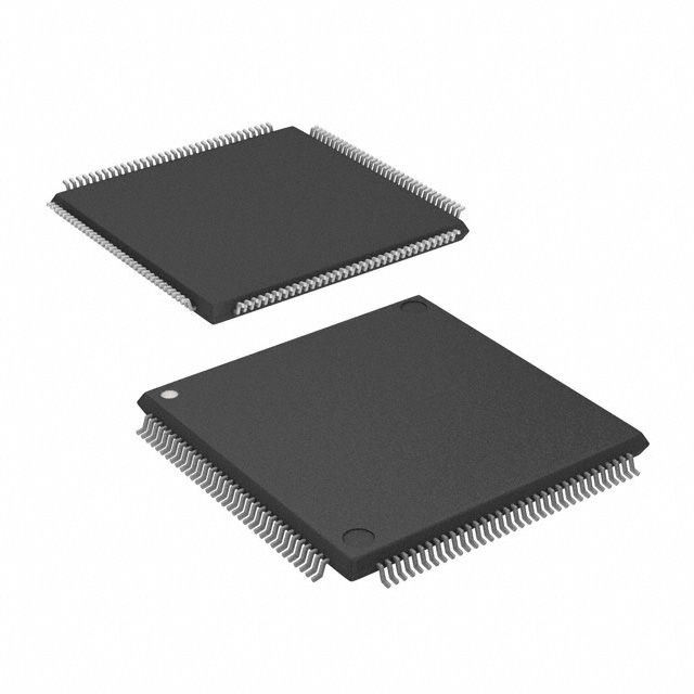
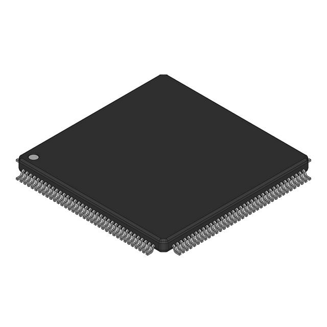
APEX-20K® Field Programmable Gate Array (FPGA) IC 101 53248 4160 144-LQFP |
|---|---|
| Quantity | 1,752 Available (as of October 8, 2026) |
| Product Category | Field Programmable Gate Array (FPGA) |
|---|---|
| Manufacturer | Intel |
| Manufacturing Status | Obsolete |
| Manufacturer Standard Lead Time | Contact Us |
| Datasheet |
Specifications & Environmental
| Device Package | 144-TQFP (20x20) | Grade | Commercial | Operating Temperature | 0°C – 85°C | ||
|---|---|---|---|---|---|---|---|
| Package / Case | 144-LQFP | Number of I/O | 101 | Voltage | 2.375 V - 2.625 V | ||
| Mounting Method | Surface Mount | RoHS Compliance | Unknown | REACH Compliance | REACH Unaffected | ||
| Moisture Sensitivity Level | 3 (168 Hours) | Number of LABs/CLBs | 416 | Number of Logic Elements/Cells | 4160 | ||
| Number of Gates | 263000 | ECCN | 3A001A2A | HTS Code | 8542.39.0001 | ||
| Qualification | N/A | Total RAM Bits | 53248 |
Overview of EP20K100TC144-3 – APEX-20K FPGA, 4,160 logic elements, ~53 kbits RAM, 144‑LQFP
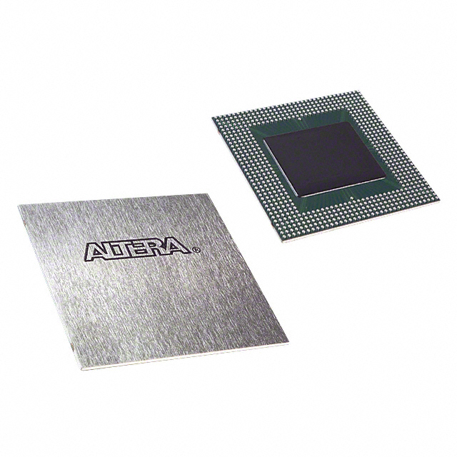
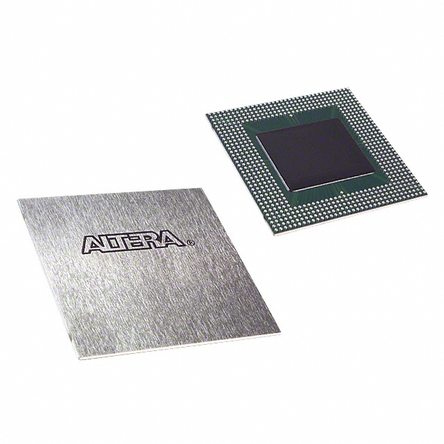
The EP20K100TC144-3 is an Intel APEX-20K series field programmable gate array (FPGA) in a 144‑LQFP package, offering a balance of logic density, embedded memory, and flexible I/O for commercial designs. Based on the APEX 20K MultiCore architecture, it integrates lookup‑table (LUT) logic, product‑term logic and embedded system blocks to implement register‑intensive and memory functions.
Targeted applications include embedded systems, high‑speed interface controllers and general-purpose programmable logic tasks where 4,160 logic elements, roughly 53,248 bits of on‑chip RAM and 101 user I/O pins provide the needed capacity and connectivity.
Key Features
- Core Architecture – APEX‑20K MultiCore architecture integrating LUT logic, product‑term logic and embedded memory for flexible implementation of combinatorial and register‑intensive functions.
- Logic Capacity – 4,160 logic elements (LEs) supporting approximately 263,000 system gates for mid‑range programmable logic designs.
- Embedded Memory – 53,248 bits of on‑chip RAM suitable for FIFOs, small buffers and local storage.
- I/O and Interfaces – 101 user I/O pins with MultiVolt I/O interface support and a programmable clamp to VCCIO; family documentation lists support for PCI and high‑speed memory interfaces (e.g., DDR SDRAM).
- Clock Management – Family features include multiple PLLs, a low‑skew clock tree and programmable clock phase/delay functions for accurate timing control.
- Power and Supply – Specified voltage supply range of 2.375 V to 2.625 V and family options for MultiVolt I/O levels; designed for low‑power operation with power‑saving modes in embedded blocks.
- Package and Thermal – 144‑LQFP surface‑mount package (supplier package 144‑TQFP, 20×20); commercial grade with an operating temperature range of 0 °C to 85 °C.
- Standards and Reliability – RoHS‑compliant component meeting commercial qualification levels listed in the product documentation.
Typical Applications
- Embedded Systems – Implement control logic, protocol handling and system‑on‑a‑chip (SOPC) functions using the device’s LUTs and embedded memory.
- High‑Speed Interface Controllers – Use the device for PCI and external memory interfacing, and for designs that require high‑performance I/O and clock management.
- Communications & Networking – Implement packet processing, buffering and protocol translation leveraging on‑chip RAM and flexible I/O standards.
- Prototyping & ASIC Emulation – Mid‑density logic and multiple I/O make the device suitable for prototype implementations and small to medium FPGA‑based proof‑of‑concepts.
Unique Advantages
- Integrated MultiCore Architecture: Combines LUT logic, product‑term logic and embedded system blocks to simplify implementation of mixed register/memory functions.
- Balanced Logic and Memory: 4,160 logic elements paired with ~53 kbits of embedded RAM provide the right mix for control, buffering and mid‑scale logic tasks.
- Flexible I/O Capability: 101 user I/Os with MultiVolt support and programmable I/O features enable straightforward interfacing across common voltage domains.
- Comprehensive Clocking: Family clock features (multiple PLLs, low‑skew clock tree, ClockBoost/ClockShift options) support complex timing requirements.
- Commercial‑Grade Reliability: Specified for 0 °C to 85 °C operation and provided in a standard surface‑mount 144‑LQFP package for easy PCB integration.
- RoHS Compliance: Environmentally compliant manufacturing and materials as noted in the product data.
Why Choose EP20K100TC144-3?
The EP20K100TC144-3 is positioned for designs that need a mid‑density FPGA with a practical balance of logic elements, embedded memory and versatile I/O in a compact 144‑LQFP footprint. Its APEX‑20K architecture and documented family features for clocking and high‑speed interfaces make it suitable for embedded controllers, interface logic and prototype systems where commercial qualification and RoHS compliance are required.
For engineers and procurement teams seeking a commercially rated APEX‑20K device with clear specification data—4,160 logic elements, 53,248 bits of RAM, 101 I/Os, and a 0 °C to 85 °C operating range—the EP20K100TC144-3 offers a straightforward, verifiable option that aligns with mid‑range programmable logic requirements.
If you would like pricing, lead time or a formal quote for the EP20K100TC144-3, request a quote or submit a product inquiry to receive current availability and ordering information.





















Date Founded: 1968
Headquarters: Santa Clara, California, USA
Employees: 130,000+
Revenue: $54.23 Billion
Certifications and Memberships: ISO9001:2015, ISO14001:2015, ISO17025:2017, ISO27001:2022, ISO45001:2018, ISO50001:2018


