
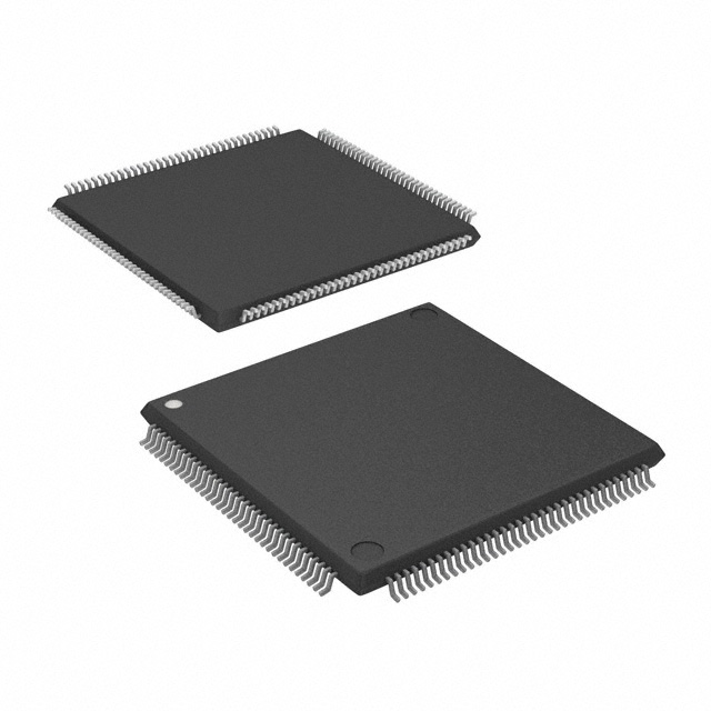
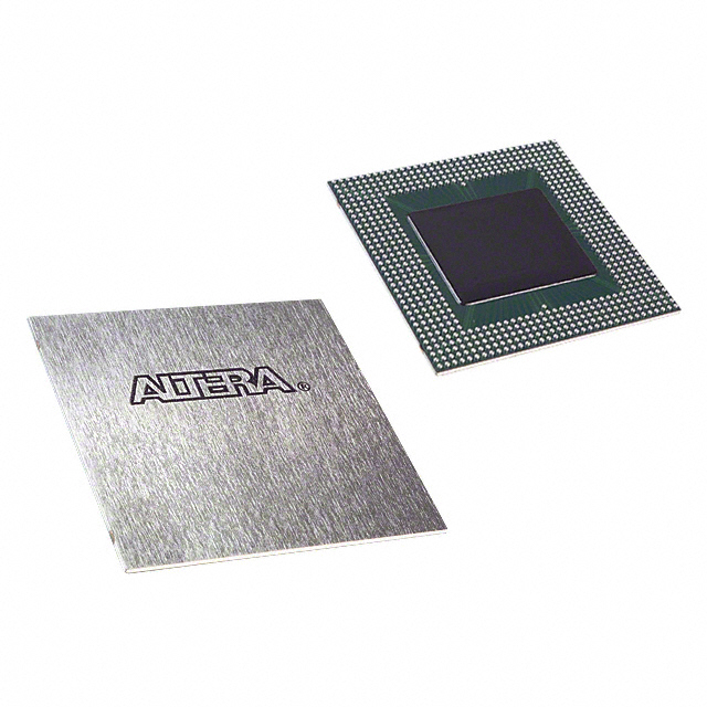
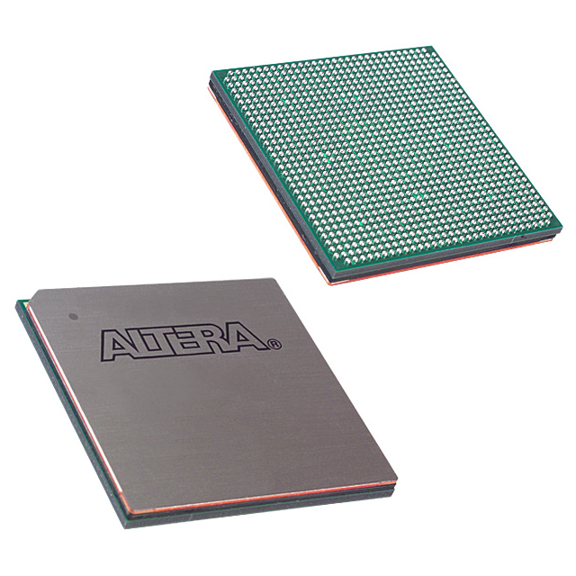
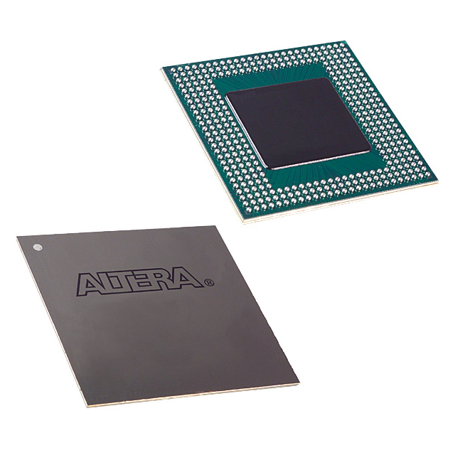
EP20K1500EBC652-1X
| Part Description |
APEX-20KE® Field Programmable Gate Array (FPGA) IC 488 442368 51840 652-BGA |
|---|---|
| Quantity | 260 Available (as of June 10, 2026) |

| Product Category | Field Programmable Gate Array (FPGA) |
|---|---|
| Manufacturer | Intel |
| Manufacturing Status | Obsolete |
| Manufacturer Standard Lead Time | Contact Us |
| Datasheet |
Specifications & Environmental
| Device Package | 652-BGA (45x45) | Grade | Commercial | Operating Temperature | 0°C – 85°C | ||
|---|---|---|---|---|---|---|---|
| Package / Case | 652-BGA | Number of I/O | 488 | Voltage | 1.71 V - 1.89 V | ||
| Mounting Method | Surface Mount | RoHS Compliance | Unknown | REACH Compliance | REACH Unaffected | ||
| Moisture Sensitivity Level | 3 (168 Hours) | Number of LABs/CLBs | 5184 | Number of Logic Elements/Cells | 51840 | ||
| Number of Gates | 2392000 | ECCN | 3A001A2A | HTS Code | 8542.39.0001 | ||
| Qualification | N/A | Total RAM Bits | 442368 |
Overview of EP20K1500EBC652-1X – APEX-20KE Field Programmable Gate Array (FPGA) 652-BGA
The EP20K1500EBC652-1X is a commercial-grade APEX-20KE family FPGA from Intel designed for system-on-programmable-chip integration. It implements a MultiCore architecture combining lookup-table (LUT) logic, product-term logic, and embedded memory blocks to support complex digital functions.
With 51,840 logic elements, approximately 0.44 Mbits of embedded memory, and 488 user I/O pins in a 652-BGA (45×45) package, this device is suited for dense logic integration, memory-centric functions, and high-pin-count interfacing in commercial embedded and communications applications.
Key Features
- Core Architecture MultiCore architecture integrating LUT logic and product-term logic for register- and combinatorial-intensive functions.
- Large Logic Capacity 51,840 logic elements and approximately 2,392,000 system gates provide high-density programmable logic for complex designs.
- Embedded Memory Approximately 442,368 RAM bits of on-chip memory for FIFOs, dual-port RAM, and CAM-style implementations without reducing available logic.
- I/O and Interface Flexibility 488 user I/O pins with MultiVolt I/O support and programmable clamp/slew-rate control to interface with multiple voltage domains.
- Clock Management Built-in clock management including up to four PLLs, low-skew clock tree, and programmable features such as ClockLock, ClockBoost, and ClockShift for flexible clocking.
- High-speed I/O Support Family-level support for high-speed interfaces and standards including LVDS performance and PCI-compliant operation for 3.3-V systems.
- Power and Supply Designed for low-power operation with a specified voltage supply range of 1.71 V to 1.89 V.
- Package and Thermal 652-ball BGA (45×45) surface-mount package; commercial operating temperature range of 0 °C to 85 °C.
- Regulatory RoHS compliant.
Typical Applications
- System Integration / SOPC Implement embedded system blocks and integrate LUT and memory resources for custom system-on-chip functions.
- Memory Interface Controllers Implement DDR SDRAM and ZBT SRAM interfaces and on-chip FIFOs using the device’s embedded memory resources.
- Bus and Bridge Logic Develop PCI-compliant 3.3-V bus interfaces and custom protocol bridges leveraging the device’s I/O capabilities.
- High-speed Data Paths Utilize LVDS-capable I/O and dedicated clock management for high-throughput signal-path and data-acquisition designs.
Unique Advantages
- Highly integrated programmable fabric: Combines LUT logic, product-term logic, and embedded system blocks to consolidate functions and reduce external components.
- Substantial on-chip memory: Approximately 0.44 Mbits of RAM enables implementation of FIFOs, buffers, and memory-centric logic without consuming logic-element capacity.
- Extensive I/O resources: 488 I/O pins and MultiVolt support simplify interfacing with multiple voltage domains and high-pin-count systems.
- Advanced clocking: Up to four PLLs plus ClockLock/ClockBoost/ClockShift features provide flexible, low-skew clock distribution for synchronous designs.
- Commercial-grade package: 652-BGA (45×45) surface-mount package supports dense board-level integration in commercial temperature environments.
- Standards-oriented I/O support: Family-level support for LVDS and PCI signaling enables ready implementation of common high-speed interfaces.
Why Choose EP20K1500EBC652-1X?
The EP20K1500EBC652-1X offers a balanced combination of high logic capacity, substantial embedded memory, and flexible I/O in a single commercial-grade FPGA package. Its MultiCore architecture and integrated system blocks make it suitable for designs that require on-chip memory, complex combinatorial and register logic, and robust clock management.
This part is well suited to engineers and teams building commercial embedded systems, interface controllers, and memory-centric logic where a high density of logic elements, versatile I/O, and programmable clock features are required. The device’s RoHS compliance and surface-mount 652-BGA package support modern PCB assembly and environmental requirements.
Request a quote or submit an inquiry to receive pricing and availability information for EP20K1500EBC652-1X.


Date Founded: 1968
Headquarters: Santa Clara, California, USA
Employees: 130,000+
Revenue: $54.23 Billion
Certifications and Memberships: ISO9001:2015, ISO14001:2015, ISO17025:2017, ISO27001:2022, ISO45001:2018, ISO50001:2018


