
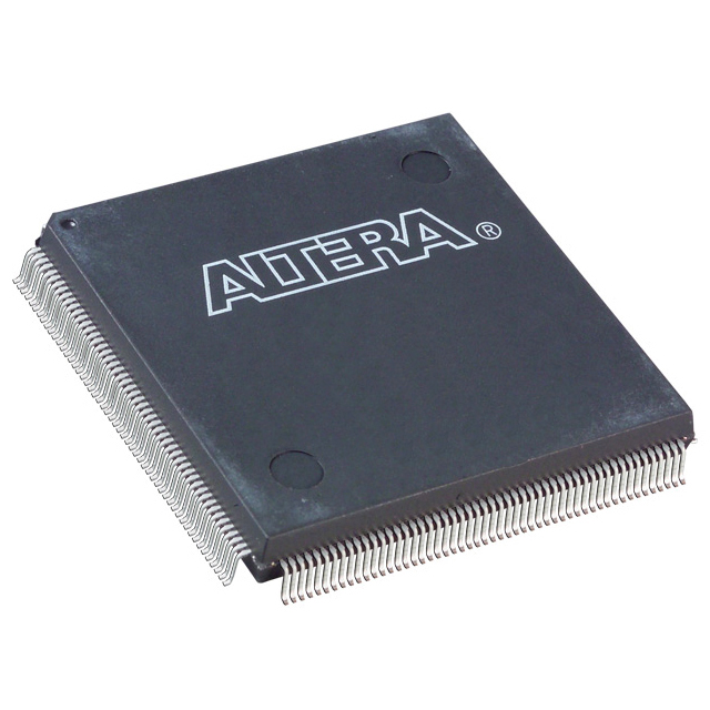
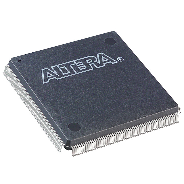
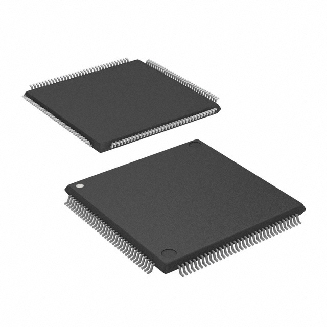
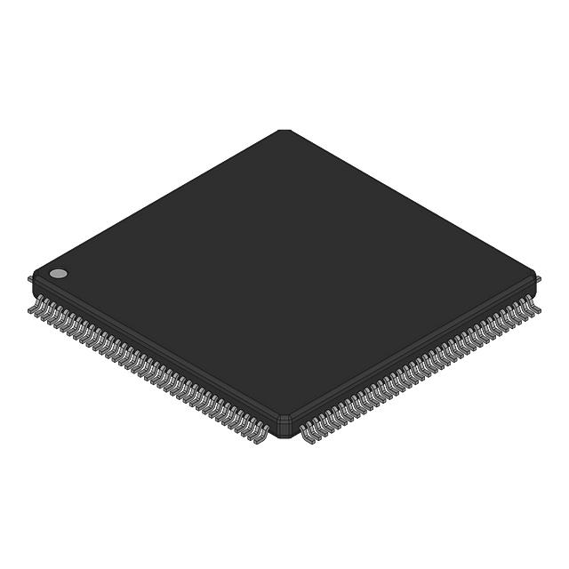
EP20K100TC144-1X
| Part Description |
APEX-20K® Field Programmable Gate Array (FPGA) IC 101 53248 4160 144-LQFP |
|---|---|
| Quantity | 260 Available (as of June 14, 2026) |

| Product Category | Field Programmable Gate Array (FPGA) |
|---|---|
| Manufacturer | Intel |
| Manufacturing Status | Obsolete |
| Manufacturer Standard Lead Time | Contact Us |
| Datasheet |
Specifications & Environmental
| Device Package | 144-TQFP (20x20) | Grade | Commercial | Operating Temperature | 0°C – 85°C | ||
|---|---|---|---|---|---|---|---|
| Package / Case | 144-LQFP | Number of I/O | 101 | Voltage | 2.375 V - 2.625 V | ||
| Mounting Method | Surface Mount | RoHS Compliance | Unknown | REACH Compliance | REACH Unaffected | ||
| Moisture Sensitivity Level | 3 (168 Hours) | Number of LABs/CLBs | 416 | Number of Logic Elements/Cells | 4160 | ||
| Number of Gates | 263000 | ECCN | 3A001A2A | HTS Code | 8542.39.0001 | ||
| Qualification | N/A | Total RAM Bits | 53248 |
Overview of EP20K100TC144-1X – APEX-20K® Field Programmable Gate Array (FPGA) IC, 101 I/O, 53,248 RAM bits, 4,160 logic elements, 144-LQFP
The EP20K100TC144-1X is an Intel APEX-20K family FPGA supplied in a 144-pin LQFP surface-mount package. It implements a MultiCore architecture that integrates look-up table (LUT) logic, product-term logic, and embedded memory blocks for compact programmable logic and memory integration.
This device targets commercial embedded designs that require moderate logic capacity, on-chip RAM, flexible I/O, and programmable clock management for system integration and custom logic functions.
Key Features
- Core architecture MultiCore architecture combining LUT logic, product-term logic, and embedded system blocks (ESBs) for implementing both register- and memory-intensive functions.
- Logic capacity 4,160 logic elements (LEs) and up to 263,000 system gates provide capacity for mid-range programmable logic tasks.
- Embedded memory Total of 53,248 on-chip RAM bits usable without reducing available logic; ESBs support FIFO, dual-port RAM, and CAM implementations.
- I/O and interface flexibility 101 user I/O pins with MultiVolt I/O interface support for 1.8 V, 2.5 V, 3.3 V, and 5.0 V signaling and programmable clamp and slew-rate control.
- Clock management Flexible clocking with up to four phase-locked loops (PLLs), built-in low-skew clock tree, and features for clock phase/delay control and multiplication/division.
- Low-power design Designed for low-power operation with support for 1.8 V and 2.5 V supply domains and ESB programmable power-saving modes.
- Advanced interconnect Four-level FastTrack® interconnect architecture and dedicated carry chain for predictable, fast interconnect delays and arithmetic performance.
- Package and mounting 144-LQFP (144-TQFP, 20×20) surface-mount package; commercial grade with operating temperature range 0 °C to 85 °C.
- Supply voltage Internal supply voltage VCCINT is 2.5 V; product supply range listed as 2.375 V to 2.625 V.
Typical Applications
- Embedded system integration Implement on-chip memory, FIFOs, and custom logic to consolidate glue logic and system functions in compact embedded platforms.
- Memory interface controllers Support for external high-speed memories and ESB memory primitives enables implementation of DDR SDRAM and ZBT SRAM interface logic.
- Custom I/O bridging and protocol glue MultiVolt I/O support and programmable I/O features make the device suitable for bridging between different voltage domains and bus standards.
- Clocked data processing Multiple PLLs and low-skew clocking support complex clocking requirements for synchronous logic and data-path designs.
Unique Advantages
- Integrated memory and logic: Embedded system blocks provide on-chip RAM and product-term logic, reducing external memory needs and BOM complexity.
- Flexible I/O voltage support: MultiVolt I/O compatibility enables direct interfacing with a range of device voltage levels without additional level-shifters.
- Programmable clocking: Up to four PLLs and clock-shifting features let designers tailor clock domains for complex timing and performance requirements.
- Predictable interconnect: Four-level FastTrack interconnect and dedicated carry chains simplify timing closure for arithmetic and routed logic paths.
- Compact surface-mount package: 144-LQFP surface-mount footprint supports PCB designs where board area and package standardization matter.
- Commercial temperature and supply support: Device is specified for commercial operating temperatures (0 °C to 85 °C) and defined supply ranges for system design planning.
Why Choose EP20K100TC144-1X?
The EP20K100TC144-1X brings APEX-20K MultiCore architecture and embedded memory into a compact 144-LQFP surface-mount package, balancing moderate logic capacity (4,160 logic elements) with 53,248 bits of on-chip RAM and 101 user I/Os. Its combination of programmable logic, ESB memory primitives, MultiVolt I/O support, and flexible clock management makes it well suited for commercial embedded designs that require integrated memory, adaptable I/O, and deterministic clocking.
For developers seeking a mid-range FPGA solution with on-chip memory and a predictable interconnect architecture, this device delivers a clear specification set for integration, board-level design, and system interfacing within commercial temperature and supply parameters.
Request a quote or submit a procurement inquiry to receive pricing and availability for the EP20K100TC144-1X and to discuss quantity, lead time, and sourcing options.


Date Founded: 1968
Headquarters: Santa Clara, California, USA
Employees: 130,000+
Revenue: $54.23 Billion
Certifications and Memberships: ISO9001:2015, ISO14001:2015, ISO17025:2017, ISO27001:2022, ISO45001:2018, ISO50001:2018


