
EP20K160EFI484-2X
| Part Description |
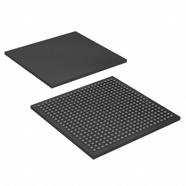
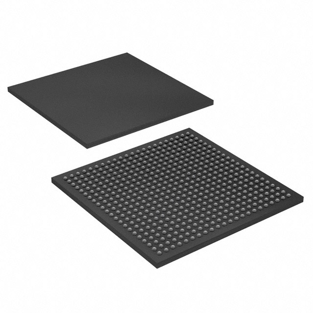
APEX-20KE® Field Programmable Gate Array (FPGA) IC 316 81920 6400 484-BBGA |
|---|---|
| Quantity | 894 Available (as of October 7, 2026) |
| Product Category | Field Programmable Gate Array (FPGA) |
|---|---|
| Manufacturer | Intel |
| Manufacturing Status | Obsolete |
| Manufacturer Standard Lead Time | Contact Us |
| Datasheet |
Specifications & Environmental
| Device Package | 484-FBGA (23x23) | Grade | Industrial | Operating Temperature | -40°C – 100°C | ||
|---|---|---|---|---|---|---|---|
| Package / Case | 484-BBGA | Number of I/O | 316 | Voltage | 1.71 V - 1.89 V | ||
| Mounting Method | Surface Mount | RoHS Compliance | Unknown | REACH Compliance | REACH Unaffected | ||
| Moisture Sensitivity Level | 3 (168 Hours) | Number of LABs/CLBs | 640 | Number of Logic Elements/Cells | 6400 | ||
| Number of Gates | 404000 | ECCN | 3A001A2A | HTS Code | 8542.39.0001 | ||
| Qualification | N/A | Total RAM Bits | 81920 |
Overview of EP20K160EFI484-2X – APEX-20KE® FPGA IC, 6,400 logic elements, 81,920 bits RAM, 316 I/O, 484-BBGA
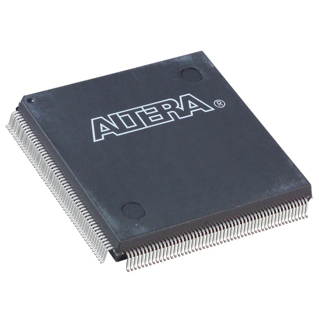
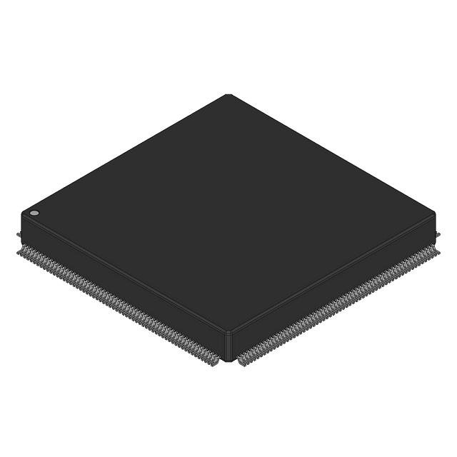
The EP20K160EFI484-2X is an APEX-20KE® field programmable gate array (FPGA) offered in a 484-BBGA surface-mount package. It implements a MultiCore architecture that integrates look-up table (LUT) logic, product-term logic and embedded memory to deliver a balanced combination of configurable logic, on-chip RAM and flexible I/O.
Targeted at designs requiring moderate-density programmable logic with industrial-temperature operation, this device supports system-level integration for interfaces, memory controllers and clock-rich applications while providing low-voltage internal operation.
Key Features
- Core architecture: MultiCore architecture combining LUT logic, product-term logic and embedded system blocks (ESBs) for register-intensive and combinatorial functions.
- Logic capacity: 6,400 logic elements, corresponding to approximately 404,000 system gates for moderate-density logic implementation.
- Embedded memory: Approximately 0.08 Mbits of embedded memory (81,920 bits) for FIFOs, dual-port RAM and CAM-style functions.
- I/O and interfacing: 316 user I/O pins with MultiVolt I/O interface support across typical APEX 20KE device levels; supports high-speed interfaces such as PCI (3.3 V operation) and LVDS capability described for the family.
- Clock management: Family features include multiple PLLs, a low-skew clock tree and programmable clock phase/delay features to support complex timing and clock distribution requirements.
- Power and supply: Designed for low-power operation; internal voltage supply specified at 1.71 V to 1.89 V for the device.
- Package and thermal: Surface-mount 484-BBGA (supplier package: 484-FBGA, 23 × 23) with operating temperature range of −40 °C to 100 °C for industrial deployment.
- On-board test and reliability: Family documentation describes integrated JTAG boundary-scan and programmable ESB features that support in-system test and configuration flows.
Typical Applications
- High-speed memory interfaces: Implement memory controllers and logic for DDR SDRAM or ZBT SRAM interfaces using on-chip memory and flexible I/O.
- PCI and bus bridging: Use the device for PCI-compliant 3.3 V bus functions and interface bridging in expansion or mezzanine card designs.
- Industrial control and automation: Deploy in industrial systems requiring programmable logic, on-chip RAM buffers and an extended −40 °C to 100 °C operating range.
- High-speed serial and differential signaling: Support LVDS channels and other high-speed I/O standards for signal conditioning and data aggregation.
Unique Advantages
- Integrated MultiCore architecture: Combines LUTs, product-term logic and ESBs to reduce external component count for memory and combinatorial functions.
- Balanced capacity for moderate-density designs: 6,400 logic elements and ~404,000 gates enable complex logic implementation without overspecifying resources.
- Flexible I/O with broad interface support: 316 user I/Os and family-level MultiVolt support enable interfacing with a wide range of voltage domains and peripheral standards.
- Industrial temperature rating: −40 °C to 100 °C operation supports deployment in demanding environments where extended temperature range is required.
- Compact BGA footprint: 484-BBGA (23 × 23) provides a space-efficient package for board-level integration while maintaining high I/O density.
- On-chip clock management: Multiple PLLs and programmable clock features simplify timing architectures for synchronous systems.
Why Choose EP20K160EFI484-2X?
The EP20K160EFI484-2X positions itself as a practical choice for engineers needing a mid-density FPGA with embedded memory, plentiful I/O and robust clock management in a compact BGA package. Its APEX-20KE family heritage provides a coherent feature set for integrating memory functions, interface logic and timing control on-chip.
With industrial temperature support and a specified internal supply range, this device suits designs that require reliable operation across temperature extremes and low-voltage internal operation while keeping system BOM and board area under control.
Request a quote or submit an inquiry to receive pricing and availability information for EP20K160EFI484-2X.





















Date Founded: 1968
Headquarters: Santa Clara, California, USA
Employees: 130,000+
Revenue: $54.23 Billion
Certifications and Memberships: ISO9001:2015, ISO14001:2015, ISO17025:2017, ISO27001:2022, ISO45001:2018, ISO50001:2018


