
EP20K30EFC256-2
| Part Description |
APEX-20KE® Field Programmable Gate Array (FPGA) IC 24576 1200 256-LBGA |
|---|---|
| Quantity | 901 Available (as of June 15, 2026) |

| Product Category | Field Programmable Gate Array (FPGA) |
|---|---|
| Manufacturer | Intel |
| Manufacturing Status | Obsolete |
| Manufacturer Standard Lead Time | Contact Us |
| Datasheet |
Specifications & Environmental
| Device Package | 256-BGA (27x27) | Grade | Commercial | Operating Temperature | 0°C – 85°C | ||
|---|---|---|---|---|---|---|---|
| Package / Case | 256-LBGA | Number of I/O | 128 | Voltage | 1.71 V - 1.89 V | ||
| Mounting Method | Surface Mount | RoHS Compliance | Unknown | REACH Compliance | REACH Unknown | ||
| Moisture Sensitivity Level | 3 (168 Hours) | Number of LABs/CLBs | 120 | Number of Logic Elements/Cells | 1200 | ||
| Number of Gates | 113000 | ECCN | OBSOLETE | HTS Code | 0000.00.0000 | ||
| Qualification | N/A | Total RAM Bits | 24576 |
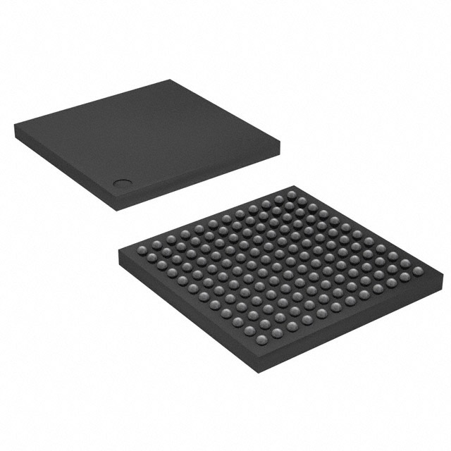
Overview of EP20K30EFC256-2 – APEX-20KE® FPGA, 1,200 logic elements, 24,576-bit embedded RAM, 256-LBGA
The EP20K30EFC256-2 is an APEX-20KE family field-programmable gate array (FPGA) in a 256-LBGA (27×27) package, optimized for commercial applications. It implements the APEX MultiCore architecture, combining look-up table (LUT) logic, product-term logic, and embedded system blocks (ESBs) to consolidate logic and memory functions on-chip.
With 1,200 logic elements, 24,576 bits of on-chip RAM, 128 user I/O pins and a commercial operating range of 0 °C to 85 °C, this device targets embedded systems and high-density logic integration where compact packaging, flexible I/O and low-power operation are important.
Key Features
- Core architecture (MultiCore) The APEX MultiCore architecture integrates LUT-based logic, product-term logic and embedded system blocks (ESBs) to implement register-intensive and memory functions on-chip.
- Logic resources 1,200 logic elements (LEs) supporting up to 113,000 system gates enables medium-density programmable logic implementations.
- Embedded memory 24,576 total RAM bits of ESB memory for FIFOs, dual-port RAM and CAM-style structures suitable for local buffering and state storage.
- I/O capability 128 user I/O pins with MultiVolt I/O interface support (family-level capability) for interfacing to a range of voltage domains and external devices.
- Clock management Family-level clock features include up to four phase-locked loops (PLLs), a built-in low-skew clock tree and provision for up to eight global clock signals to simplify timing distribution.
- Power and voltage Internal supply and device operation targeted around 1.8 V (specified voltage supply range 1.71 V to 1.89 V), with family features for programmable power-saving modes.
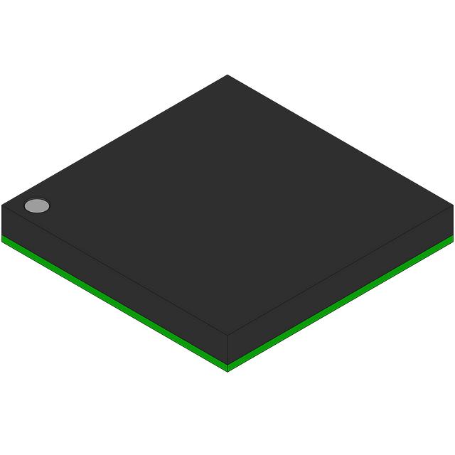
- Package and mounting 256-LBGA (27×27) surface-mount package providing a compact footprint for space-constrained PCBs.
- Commercial grade and compliance Commercial operating temperature range 0 °C to 85 °C and RoHS-compliant manufacturing.
Typical Applications
- Embedded control and processing On-chip LUT logic and ESB memory enable control state machines, protocol handling and local buffering in embedded systems.
- High-speed interfaces and bridging MultiVolt I/O support and family-level I/O features help implement interface bridging and protocol adaptation between different voltage domains.
- Memory interfacing and buffering ESB RAM and dedicated interconnect support use as local FIFOs and memory controllers for external memory interfaces.
- Communication endpoints Programmable clock management and flexible I/O are suitable for mid-range communication endpoints requiring deterministic clocking and moderate I/O counts.
Unique Advantages
- Integrated logic and memory: The MultiCore architecture with ESBs consolidates logic and RAM on-chip, reducing external component count for buffering and state storage.
- Balanced resource mix: 1,200 logic elements paired with 24,576 bits of embedded RAM and 128 I/O pins offers a practical balance for medium-density designs.
- Flexible clocking: Family-level PLLs and multiple global clocks simplify implementation of complex timing domains and reduce board-level clocking requirements.
- Compact, surface-mount package: The 256-LBGA (27×27) package enables high-density PCB layouts while maintaining robust I/O connectivity.
- Commercial temperature and RoHS compliance: Specified 0 °C to 85 °C operation and RoHS compliance support mainstream commercial product development and manufacturing requirements.
Why Choose EP20K30EFC256-2?
The EP20K30EFC256-2 positions itself as a mid-density, commercial-grade FPGA option within the APEX-20K family, offering a practical combination of logic elements, embedded RAM and I/O for embedded designs. Its MultiCore architecture and family-level clock and I/O features provide the on-chip integration designers need to reduce external components and simplify board-level design.
This device is well suited for developers seeking a commercially-rated FPGA from the APEX-20K family with compact 256-LBGA packaging, low-power design considerations and clearly specified logic and memory resources for medium-complexity applications.
Request a quote or submit a pricing inquiry for EP20K30EFC256-2 to receive availability and lead-time information for your project needs.


Date Founded: 1968
Headquarters: Santa Clara, California, USA
Employees: 130,000+
Revenue: $54.23 Billion
Certifications and Memberships: ISO9001:2015, ISO14001:2015, ISO17025:2017, ISO27001:2022, ISO45001:2018, ISO50001:2018


