
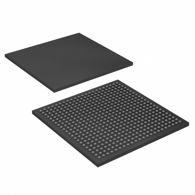
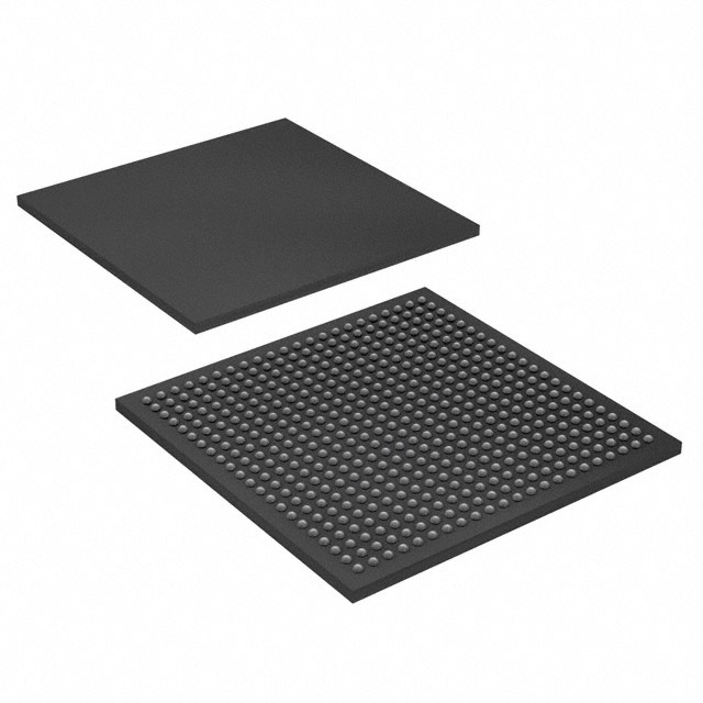
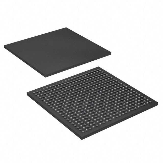
EP2C50U484C7N
| Part Description |
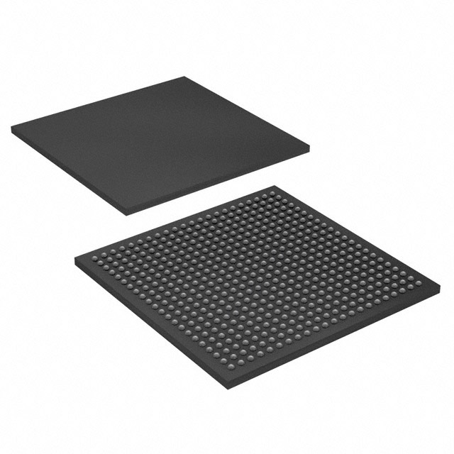
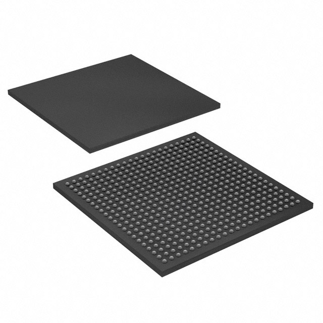
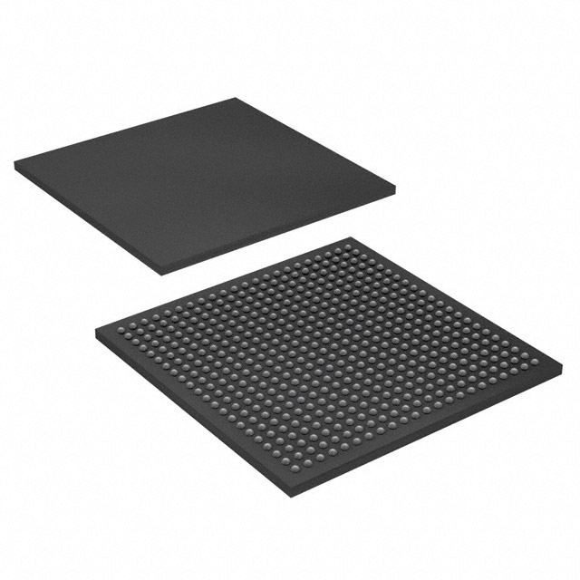
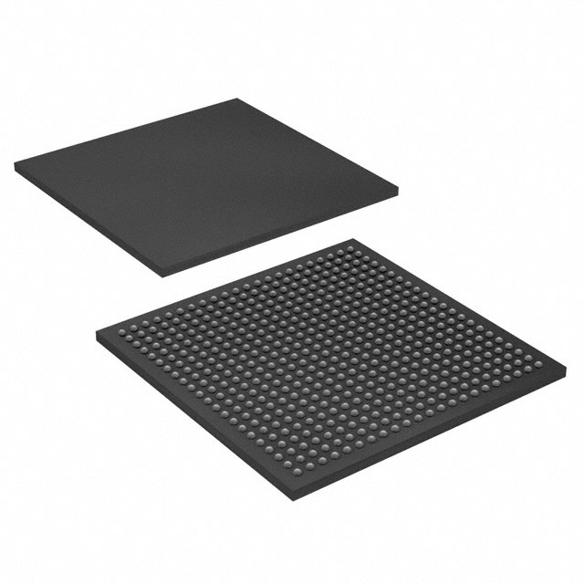
Cyclone® II Field Programmable Gate Array (FPGA) IC 294 594432 50528 484-FBGA |
|---|---|
| Quantity | 1,284 Available (as of October 8, 2026) |
| Product Category | Field Programmable Gate Array (FPGA) |
|---|---|
| Manufacturer | Intel |
| Manufacturing Status | Active |
| Manufacturer Standard Lead Time | 26 Weeks |
| Datasheet |
Specifications & Environmental
| Device Package | 484-UBGA (19x19) | Grade | Commercial | Operating Temperature | 0°C – 85°C | ||
|---|---|---|---|---|---|---|---|
| Package / Case | 484-FBGA | Number of I/O | 294 | Voltage | 1.15 V - 1.25 V | ||
| Mounting Method | Surface Mount | RoHS Compliance | RoHS Compliant | REACH Compliance | REACH Unaffected | ||
| Moisture Sensitivity Level | 3 (168 Hours) | Number of LABs/CLBs | 3158 | Number of Logic Elements/Cells | 50528 | ||
| Number of Gates | N/A | ECCN | 3A991D | HTS Code | 8542.39.0001 | ||
| Qualification | N/A | Total RAM Bits | 594432 |
Overview of EP2C50U484C7N – Cyclone® II Field Programmable Gate Array (FPGA) IC 294 594432 50528 484-FBGA
The EP2C50U484C7N is a Cyclone® II family FPGA from Intel, offered in a 484-FBGA package for surface-mount applications. Designed for low-cost embedded processing and DSP-focused designs, this device combines a large logic fabric with embedded memory and flexible I/O resources.
As a member of the Cyclone II device family, the part is documented in the Cyclone II device handbook and provides architecture-level features such as a global clock network with PLLs, embedded multipliers, and dedicated memory blocks to support configurable digital logic, signal processing, and external memory interfacing.
Key Features
- Logic Capacity — 50,528 logic elements to implement complex custom logic and state machines.
- Embedded Memory — Approximately 0.59 Mbits of on-chip RAM (594,432 total RAM bits) for buffering, lookup tables, and packet or frame storage.
- I/O Resources — 294 I/O pins with advanced I/O support, programmable drive strength, programmable pull-ups, and options for differential signaling.
- Dedicated DSP Resources — Embedded multipliers and routing optimized for arithmetic and digital signal processing paths as documented in the Cyclone II handbook.
- Clocking and PLLs — Global clock network and phase-locked loops (PLLs) for flexible clocking, distribution, and phase control across the device.
- Power and Voltage — Core voltage supply range of 1.15 V to 1.25 V to match Cyclone II core requirements.
- Package and Mounting — 484-FBGA (supplier package 484-UBGA, 19 × 19) surface-mount package suitable for compact board designs.
- Commercial Grade & Compliance — Commercial operating temperature range of 0 °C to 85 °C and RoHS-compliant.
Typical Applications
- Low-Cost Embedded Processing — Implement microcontroller-style logic, glue logic, and control functions where cost-sensitive FPGA solutions are required.
- Low-Cost DSP Solutions — Leverage embedded multipliers and on-chip RAM for signal filtering, transforms, and other DSP workloads at lower system cost.
- Memory and Interface Bridging — Use flexible I/O and external memory interfacing capabilities for protocol bridging, buffering, and custom interface implementations.
Unique Advantages
- High Logic Density: 50,528 logic elements provide headroom for complex designs and multiple concurrent functions on a single device.
- Significant On-Chip RAM: Approximately 0.59 Mbits of embedded memory reduces dependence on external memory for many buffering and LUT needs.
- Rich I/O Count and Flexibility: 294 I/Os with programmable drive and advanced I/O standard support simplify board-level integration and signal conditioning.
- Built-In DSP Primitives: Embedded multipliers and optimized routing help accelerate arithmetic-heavy tasks without external accelerators.
- Flexible Clocking: Global clock network and PLLs enable robust clock distribution and multiple clock domains within a single design.
- Compact, Surface-Mount Package: 484-FBGA (19 × 19) package supports dense PCB layouts while maintaining a high pin count.
Why Choose EP2C50U484C7N?
The EP2C50U484C7N integrates substantial logic, on-chip RAM, DSP resources, and a high-density I/O set in a commercially graded Cyclone II FPGA package. It is positioned for engineers building cost-sensitive embedded and DSP-enabled systems who need a balance of capacity, configurable I/O, and on-chip resources documented in the Cyclone II device handbook.
This part is suited to designs that require scalable logic capacity, flexible clocking and interface options, and the support of established device documentation and development flows within the Cyclone II family.
Request a quote or submit a pricing and availability request to get component pricing, lead time, and ordering details for EP2C50U484C7N.





















Date Founded: 1968
Headquarters: Santa Clara, California, USA
Employees: 130,000+
Revenue: $54.23 Billion
Certifications and Memberships: ISO9001:2015, ISO14001:2015, ISO17025:2017, ISO27001:2022, ISO45001:2018, ISO50001:2018


