
EP2C50U484C8
| Part Description |
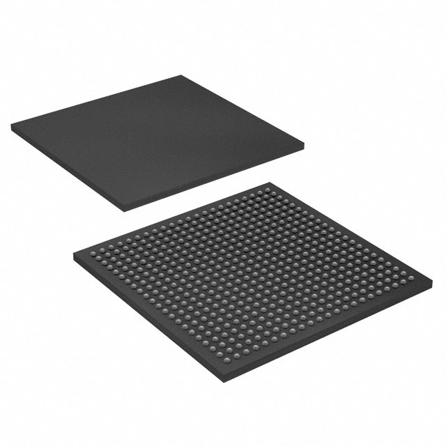
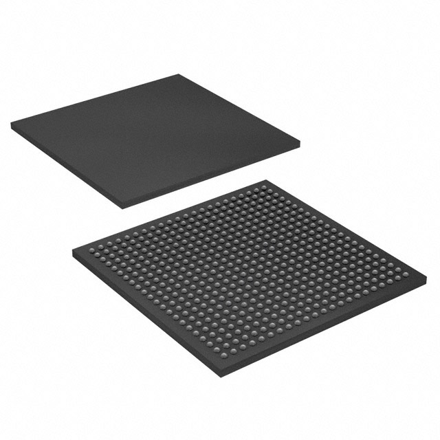
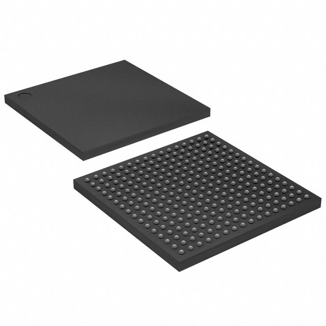
Cyclone® II Field Programmable Gate Array (FPGA) IC 294 594432 50528 484-FBGA |
|---|---|
| Quantity | 113 Available (as of October 8, 2026) |
| Product Category | Field Programmable Gate Array (FPGA) |
|---|---|
| Manufacturer | Intel |
| Manufacturing Status | Active |
| Manufacturer Standard Lead Time | 26 Weeks |
| Datasheet |
Specifications & Environmental
| Device Package | 484-UBGA (19x19) | Grade | Commercial | Operating Temperature | 0°C – 85°C | ||
|---|---|---|---|---|---|---|---|
| Package / Case | 484-FBGA | Number of I/O | 294 | Voltage | 1.15 V - 1.25 V | ||
| Mounting Method | Surface Mount | RoHS Compliance | RoHS Compliant | REACH Compliance | REACH Unaffected | ||
| Moisture Sensitivity Level | 3 (168 Hours) | Number of LABs/CLBs | 3158 | Number of Logic Elements/Cells | 50528 | ||
| Number of Gates | N/A | ECCN | 3A991D | HTS Code | 8542.39.0001 | ||
| Qualification | N/A | Total RAM Bits | 594432 |
Overview of EP2C50U484C8 – Cyclone® II Field Programmable Gate Array (FPGA) IC 294 594432 50528 484-FBGA
The EP2C50U484C8 is an Intel Cyclone® II FPGA offered in a 484-ball FBGA package, designed for low-cost embedded processing and DSP-oriented applications. It combines a high logic capacity with abundant I/O and on-chip memory to support system integration where cost, power efficiency, and moderate performance are priorities.
This device targets commercial-grade applications that require flexible logic resources, multiple interface options, and a compact surface-mount package with a core voltage supply between 1.15 V and 1.25 V and an operating temperature range of 0 °C to 85 °C.
Key Features
- Logic Capacity — 50,528 logic elements organized across 3,158 LABs, enabling implementation of complex combinational and sequential logic functions.
- Embedded Memory — Approximately 0.57 Mbits of on-chip RAM (594,432 total RAM bits) for FIFOs, buffers, and local storage to support embedded processing and data buffering.
- I/O and Interface Flexibility — 294 user I/O pins with documented I/O structure and programmable drive features to support a variety of single-ended and differential interfaces and external memory connections.
- Clocking and Timing — Dedicated global clock network and Phase-Locked Loop (PLL) resources for disciplined clock distribution and timing control across the design.
- Embedded DSP Resources — Integrated embedded multipliers and dedicated routing to support DSP and arithmetic-intensive functions within the Cyclone II architecture.
- Package and Mounting — Surface-mount 484-FBGA package (supplier package: 484-UBGA, 19×19) for space-constrained board designs.
- Power and Thermal — Supported core supply voltage range of 1.15 V to 1.25 V and a commercial operating temperature range of 0 °C to 85 °C.
- Standards and Compliance — RoHS-compliant manufacturing and materials.
Typical Applications
- Embedded Processing — Implement soft processors, control logic, and glue-logic functions using the device’s logic elements and on-chip memory for compact system designs.
- DSP and Signal Processing — Use embedded multipliers and dedicated routing to implement filtering, transforms, and arithmetic pipelines for moderate-performance DSP tasks.
- Interface Bridging — Leverage 294 I/Os and programmable I/O features to connect disparate peripherals, external memory, or communication interfaces.
- Memory Interfacing — Use the device’s external memory interfacing capabilities and on-chip RAM to implement buffering and controller logic for external memory subsystems.
Unique Advantages
- High Logic Density: 50,528 logic elements provide substantial capacity to consolidate multiple functions into a single FPGA, reducing PCB BOM and board area.
- Integrated Memory Resources: Approximately 0.57 Mbits of embedded RAM allow local data storage and buffering without immediate reliance on external memory.
- Extensive I/O Count: 294 I/O pins support complex multi-channel interfaces and give designers flexibility in system partitioning.
- Dedicated Clocking and PLLs: Global clock network and PLL resources enable controlled clock distribution and frequency synthesis for synchronous designs.
- Compact, Surface-Mount Package: The 484-FBGA (484-UBGA, 19×19) form factor suits space-constrained assemblies while providing a high pin count.
- Regulatory and Manufacturing Readiness: RoHS-compliant construction supports environmental and production requirements for commercial applications.
Why Choose EP2C50U484C8?
The EP2C50U484C8 positions itself as a cost-conscious Cyclone II FPGA option that balances sizable logic resources, embedded memory, and flexible I/O in a compact FBGA package. Its combination of 50,528 logic elements, substantial on-chip RAM, and dedicated DSP and clocking features makes it suitable for designers consolidating control, interface, and moderate DSP functions into a single programmable device.
This device is well suited to commercial embedded designs that require scalable logic capacity, routine operating temperature support, and RoHS compliance. It provides a reliable platform for teams looking to optimize board-level integration while leveraging the Cyclone II device family architecture and documentation.
If you would like pricing, availability, or to request a quote for the EP2C50U484C8, please submit your request and a sales representative will respond with details and next steps.





















Date Founded: 1968
Headquarters: Santa Clara, California, USA
Employees: 130,000+
Revenue: $54.23 Billion
Certifications and Memberships: ISO9001:2015, ISO14001:2015, ISO17025:2017, ISO27001:2022, ISO45001:2018, ISO50001:2018


