
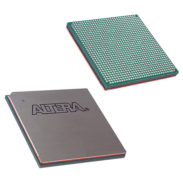
EP2S130F1020C3N
| Part Description |
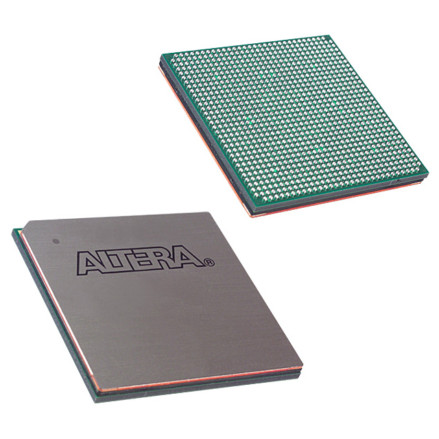
Stratix® II Field Programmable Gate Array (FPGA) IC 742 6747840 132540 1020-BBGA |
|---|---|
| Quantity | 460 Available (as of October 8, 2026) |
| Product Category | Field Programmable Gate Array (FPGA) |
|---|---|
| Manufacturer | Intel |
| Manufacturing Status | Obsolete |
| Manufacturer Standard Lead Time | Contact Us |
| Datasheet |
Specifications & Environmental
| Device Package | 1020-FBGA (33x33) | Grade | Commercial | Operating Temperature | 0°C – 85°C | ||
|---|---|---|---|---|---|---|---|
| Package / Case | 1020-BBGA | Number of I/O | 742 | Voltage | 1.15 V - 1.25 V | ||
| Mounting Method | Surface Mount | RoHS Compliance | RoHS Compliant | REACH Compliance | REACH Unaffected | ||
| Moisture Sensitivity Level | 3 (168 Hours) | Number of LABs/CLBs | 6627 | Number of Logic Elements/Cells | 132540 | ||
| Number of Gates | N/A | ECCN | 3A001A7A | HTS Code | 8542.39.0001 | ||
| Qualification | N/A | Total RAM Bits | 6747840 |
Overview of EP2S130F1020C3N – Stratix® II Field Programmable Gate Array, 1020-BBGA
The EP2S130F1020C3N is a Stratix II field programmable gate array (FPGA) in a 1020-ball BGA package. It delivers a high-capacity programmable logic fabric with embedded memory and extensive I/O, suitable for complex digital designs and system integration tasks.
Designed for commercial applications, this device combines a large logic element count, significant on-chip RAM, and support features described in the Stratix II device handbook (architecture, PLLs, DSP blocks, configuration and I/O capabilities), enabling flexible implementation of custom logic, memory interfaces and high-density I/O subsystems.
Key Features
- Logic Capacity 132,540 logic elements (adaptive logic modules and LAB organization as described in the Stratix II handbook) to implement complex custom logic and state machines.
- Embedded Memory Approximately 6.75 Mbits of on-chip RAM for buffering, FIFOs, and local data storage.
- Large I/O Count 742 I/O pins to support wide data buses, multiple interfaces and dense board-level connectivity.
- Clocking & DSP Resources Stratix II family features such as PLLs, enhanced and fast PLL options, and digital signal processing blocks (documented in the device handbook) for flexible clock management and DSP-oriented datapaths.
- Configuration & Debug Support Configuration options, JTAG boundary-scan support and the SignalTap II embedded logic analyzer are part of the documented Stratix II feature set to aid bring-up and debug.
- Power Supply Requires core supply in the range of 1.15 V to 1.25 V, supporting the power domains specified for Stratix II devices.
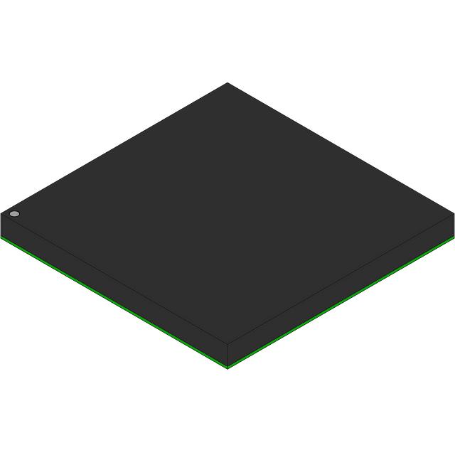
- Package & Mounting 1020-BBGA (supplier package specified as 1020-FBGA, 33×33) in a surface-mount form factor for compact, high-pin-count designs.
- Commercial Temperature Grade Rated for 0 °C to 85 °C operating temperature, for commercial-environment deployments.
- Regulatory Compliance RoHS compliant.
Typical Applications
- High-density digital systems Implement large custom logic networks, protocol conversion, or complex state machines using the device’s 132,540 logic elements and on-chip memory.
- Memory interface and buffering Use the approximately 6.75 Mbits of embedded RAM and documented TriMatrix memory architecture to create memory controllers, buffers and arbitration logic for external RAM interfacing.
- Signal processing and interface bridging Leverage the Stratix II DSP blocks and PLLs (as described in the device handbook) for DSP datapaths, clock management, and high-speed serial or parallel interface implementations.
- Prototyping and system integration Dense I/O (742 pins) and extensive configuration/debug support make the device suitable for hardware prototypes and integration of multiple subsystems on a single FPGA.
Unique Advantages
- High logic density: 132,540 logic elements provide the capacity to consolidate multiple functions into a single device, reducing board-level complexity.
- Substantial on-chip memory: Approximately 6.75 Mbits of embedded RAM reduces dependence on external memory for many buffering and storage tasks.
- Extensive I/O integration: 742 I/Os enable broad connectivity options for interfacing with parallel buses, external peripherals and multi-channel systems.
- Flexible clocking and DSP capabilities: Family-level features such as enhanced/fast PLLs and DSP blocks support a range of timing and signal-processing architectures.
- Commercial-grade robustness: Rated for 0 °C to 85 °C operating temperature and RoHS compliant for commercial deployments.
- Compact high-pin-count package: 1020-BBGA (33×33 supplier package) provides a balance of pin density and board-area efficiency for space-constrained designs.
Why Choose EP2S130F1020C3N?
The EP2S130F1020C3N positions itself as a high-capacity Stratix II FPGA option for commercial applications that require large programmable logic resources, significant embedded memory, and broad I/O connectivity. It is suitable for engineers consolidating multiple functions into a single programmable device, implementing complex memory interfaces, or building DSP-forward datapaths using the Stratix II architectural features documented in the device handbook.
Backed by the Stratix II device documentation from Altera/Intel, this device is a practical choice for designs that prioritize integration density, configurable logic capacity and documented configuration and debug capabilities. Its package, voltage and temperature specifications make it compatible with commercial production boards and standard surface-mount assembly flows.
If you need pricing, availability or a formal quote for EP2S130F1020C3N, request a quote or submit a quote request with your quantity and required delivery timeline.




















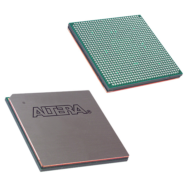



Date Founded: 1968
Headquarters: Santa Clara, California, USA
Employees: 130,000+
Revenue: $54.23 Billion
Certifications and Memberships: ISO9001:2015, ISO14001:2015, ISO17025:2017, ISO27001:2022, ISO45001:2018, ISO50001:2018


