
EP4SGX180KF40I3
| Part Description |
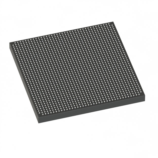
Stratix® IV GX Field Programmable Gate Array (FPGA) IC 744 13954048 175750 1517-BBGA, FCBGA |
|---|---|
| Quantity | 1,114 Available (as of October 8, 2026) |
| Product Category | Field Programmable Gate Array (FPGA) |
|---|---|
| Manufacturer | Intel |
| Manufacturing Status | Obsolete |
| Manufacturer Standard Lead Time | Contact Us |
| Datasheet |
Specifications & Environmental
| Device Package | 1517-FBGA (40x40) | Grade | Industrial | Operating Temperature | -40°C – 100°C | ||
|---|---|---|---|---|---|---|---|
| Package / Case | 1517-BBGA, FCBGA | Number of I/O | 744 | Voltage | 870 mV - 930 mV | ||
| Mounting Method | Surface Mount | RoHS Compliance | RoHS non-compliant | REACH Compliance | REACH Unknown | ||
| Moisture Sensitivity Level | 3 (168 Hours) | Number of LABs/CLBs | 7030 | Number of Logic Elements/Cells | 175750 | ||
| Number of Gates | N/A | ECCN | 3A001A7A | HTS Code | 8542.39.0001 | ||
| Qualification | N/A | Total RAM Bits | 13954048 |
Overview of EP4SGX180KF40I3 – Stratix® IV GX FPGA IC, 175,750 logic elements, 744 I/O
The EP4SGX180KF40I3 is an Intel Stratix® IV GX field programmable gate array supplied in a 1517‑BBGA (FCBGA) package for surface‑mount applications. The device integrates high logic density, substantial embedded memory, and architecture features from the Stratix IV family to address designs that require large-scale programmable logic and extensive I/O capability.
Targeted at industrial applications, this device delivers a combination of logic capacity, on‑chip RAM and high‑speed I/O building blocks suitable for demanding communications and data‑processing tasks while supporting an extended operating temperature range.
Key Features
- FPGA Core 175,750 logic elements providing the programmable fabric necessary for complex digital designs and high‑density logic integration.
- Embedded Memory Approximately 13.95 Mbits of on‑chip RAM to support buffering, packet processing, and local data storage requirements.
- I/O Capacity 744 I/O pins to accommodate wide bus interfaces, multi‑port peripherals, and extensive external connectivity.
- High‑Speed Transceiver and I/O Features Includes Stratix IV GX device family transceiver and high‑speed differential I/O capabilities as described in the device handbook (DPA and Soft‑CDR referenced for differential I/O handling).
- Clocking and Timing Integrated clock networks and PLL resources are part of the Stratix IV architecture to manage multi‑clock domains and high‑performance timing requirements.
- DSP and System Blocks Device family documentation notes dedicated DSP blocks and system integration features for signal processing and protocol support.
- Package & Mounting 1517‑BBGA (FCBGA) supplier package: 1517‑FBGA (40×40); surface‑mount package suitable for board‑level integration.
- Supply & Temperature Core voltage range: 870 mV to 930 mV. Operating temperature: −40 °C to 100 °C, supporting industrial temperature environments.
- Regulatory RoHS compliant.
Typical Applications
- High‑performance networking and communications Use the device’s large logic capacity, abundant I/O, and Stratix IV GX transceiver features to implement protocol processing, packet switching, and interface bridging.
- Telecom and data‑plane processing On‑chip RAM and DSP resources support buffering, classification, and real‑time data manipulation in telecom equipment.
- Industrial control and automation Industrial temperature rating and extensive I/O enable complex control logic, sensor aggregation, and deterministic I/O handling in industrial systems.
- High‑speed data acquisition and processing Large logic fabric and embedded memory facilitate front‑end data conditioning, aggregation, and preprocessing for downstream systems.
Unique Advantages
- High logic density: 175,750 logic elements let you consolidate multiple functions into a single device, reducing board-level BOM and interconnect complexity.
- Significant on‑chip memory: Approximately 13.95 Mbits of embedded RAM supports large buffers and on‑device data processing without immediate reliance on external memory.
- Extensive I/O connectivity: 744 I/O pins give flexibility to interface with multiple high‑pin‑count peripherals and bus standards simultaneously.
- Industrial temperature range: Rated from −40 °C to 100 °C for reliable operation in a wide range of environmental conditions.
- Stratix IV GX family feature set: Architecture elements documented in the Stratix IV device handbook — including high‑speed transceivers, DSP blocks, PLLs and clock networks — provide a foundation for high‑bandwidth and protocol‑rich designs.
- Surface‑mount, high‑density package: 1517‑BBGA FCBGA (40×40) package enables compact board layouts while supporting large I/O counts.
Why Choose EP4SGX180KF40I3?
The EP4SGX180KF40I3 combines substantial programmable logic capacity, sizable embedded memory, and the Stratix IV GX family’s high‑speed I/O and transceiver feature set to serve designs that demand high integration and throughput. Its industrial temperature rating and RoHS compliance make it suitable for production deployments that require robustness and regulatory alignment.
This device is well suited to engineering teams building complex communications, data‑processing, and industrial control systems that need scalable FPGA resources, broad I/O, and the documented architecture features of the Stratix IV family.
Request a quote or submit an inquiry to receive pricing and availability information for the EP4SGX180KF40I3 and begin integrating this Stratix IV GX FPGA into your next high‑performance design.























Date Founded: 1968
Headquarters: Santa Clara, California, USA
Employees: 130,000+
Revenue: $54.23 Billion
Certifications and Memberships: ISO9001:2015, ISO14001:2015, ISO17025:2017, ISO27001:2022, ISO45001:2018, ISO50001:2018


