
EP4SGX70HF35C3G
| Part Description |
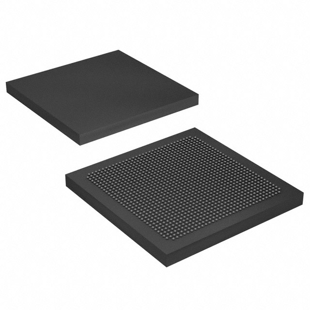
Stratix® IV GX Field Programmable Gate Array (FPGA) IC 488 7564880 72600 1152-BBGA, FCBGA |
|---|---|
| Quantity | 1,044 Available (as of June 18, 2026) |

| Product Category | Field Programmable Gate Array (FPGA) |
|---|---|
| Manufacturer | Intel |
| Manufacturing Status | Active |
| Manufacturer Standard Lead Time | 26 Weeks |
| Datasheet |
Specifications & Environmental
| Device Package | 1152-FBGA (35x35) | Grade | Commercial | Operating Temperature | 0°C – 85°C | ||
|---|---|---|---|---|---|---|---|
| Package / Case | 1152-BBGA, FCBGA | Number of I/O | 488 | Voltage | 870 mV - 930 mV | ||
| Mounting Method | Surface Mount | RoHS Compliance | RoHS Compliant | REACH Compliance | REACH Unaffected | ||
| Moisture Sensitivity Level | 3 (168 Hours) | Number of LABs/CLBs | 2904 | Number of Logic Elements/Cells | 72600 | ||
| Number of Gates | N/A | ECCN | PENDING ECCN | HTS Code | 0000.00.0000 | ||
| Qualification | N/A | Total RAM Bits | 7564880 |
Overview of EP4SGX70HF35C3G – Stratix® IV GX FPGA, 1152‑FBGA (35×35), 488 I/O
The EP4SGX70HF35C3G is a Stratix® IV GX Field Programmable Gate Array (FPGA) IC optimized for high‑bandwidth digital designs. Based on the Stratix IV device family architecture, it combines a dense logic fabric with substantial on‑chip memory and extensive I/O to address demanding signal‑processing and high‑speed serial interface requirements.
Designed for commercial applications, this device targets system designs that require large logic capacity, embedded RAM, and configurable high‑speed interfaces while offering surface‑mount placement in a 1152‑FBGA package.
Key Features
- Logic Capacity — 72,600 logic elements provide substantial programmable logic for complex FPGA implementations.
- Embedded Memory — Approximately 7.56 Mbits of on‑chip RAM for buffering, look‑up tables, and memory‑intensive functions.
- I/O Density — 488 I/O pins to support wide external interfacing and parallel data paths.
- High‑Performance Architecture — Stratix IV GX family features including DSP block support, clock networks and PLLs as documented in the Stratix IV device handbook for building high‑throughput designs.
- High‑Speed Transceiver Capability — Family‑level transceiver and high‑speed differential I/O features (referenced in the device handbook) support implementation of serial protocols and high aggregate data bandwidth.
- Power Requirements — Core voltage supply range of 870 mV to 930 mV, enabling predictable power budgeting for system design.
- Package & Mounting — 1152‑FBGA (35×35 mm) FCBGA package; surface‑mount mounting type suitable for compact board layouts.
- Commercial Grade & Temperature — Commercial grade device rated for 0 °C to 85 °C operation.
- Compliance — RoHS compliant.
Typical Applications
- High‑speed serial interfaces — Use the device’s Stratix IV GX family transceiver features and abundant I/O to implement multi‑lane serial links and protocol bridging.
- Digital signal processing — Leverage the device’s logic capacity and embedded memory for DSP pipelines, filters, and real‑time data manipulation.
- External memory controllers — Implement external memory interfaces and buffering with the available on‑chip RAM and robust clocking resources.
- Data aggregation and switching — High I/O count and large logic fabric support packet processing, aggregation, and custom switching functions.
Unique Advantages
- Substantial logic resources: 72,600 logic elements enable complex, highly parallel designs without repartitioning.
- Significant embedded RAM: Approximately 7.56 Mbits of on‑chip memory reduces dependence on external RAM for many buffering and LUT needs.
- High I/O flexibility: 488 general‑purpose I/Os allow broad interfacing options and support for parallel and serial system architectures.
- Family‑level high‑speed features: Stratix IV GX architecture provides transceiver and signal‑integrity capabilities described in the device handbook, aiding high‑bandwidth protocol implementations.
- Compact system footprint: 1152‑FBGA, surface‑mount package consolidates high capacity in a board‑space efficient form factor.
- Regulatory and procurement simplicity: RoHS compliance supports modern manufacturing requirements for commercial products.
Why Choose EP4SGX70HF35C3G?
The EP4SGX70HF35C3G delivers a balance of logic density, embedded memory, and extensive I/O in the Stratix IV GX family architecture, making it well suited for designers building high‑bandwidth, compute‑intensive systems. Its commercial‑grade rating, defined operating temperature range, and documented family features such as DSP blocks, clock networks, PLLs, and high‑speed transceiver capability provide a verified platform for scalable, performance‑oriented FPGA designs.
This part is appropriate for engineering teams that need a proven FPGA fabric with on‑chip memory and a high pin count in a compact FCBGA package, supported by the Stratix IV device handbook and vendor documentation for system integration and design planning.
Request a quote or submit an RFQ today to get pricing and availability details for EP4SGX70HF35C3G.


Date Founded: 1968
Headquarters: Santa Clara, California, USA
Employees: 130,000+
Revenue: $54.23 Billion
Certifications and Memberships: ISO9001:2015, ISO14001:2015, ISO17025:2017, ISO27001:2022, ISO45001:2018, ISO50001:2018


