
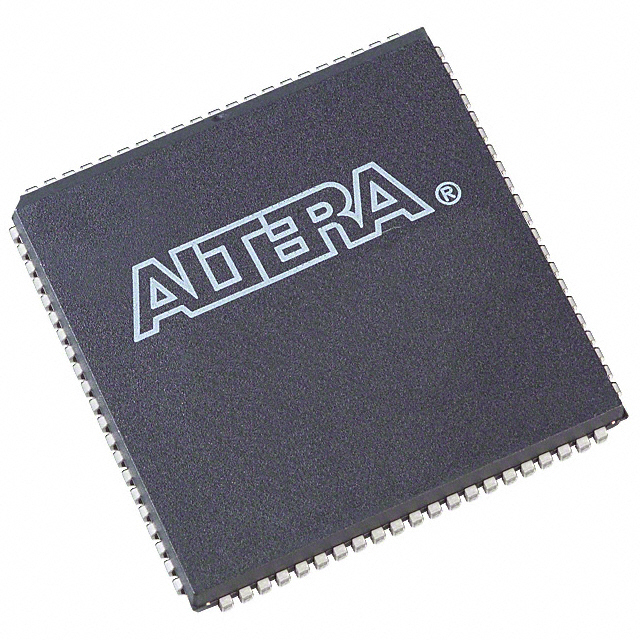
EPF10K10LC84-3
| Part Description |
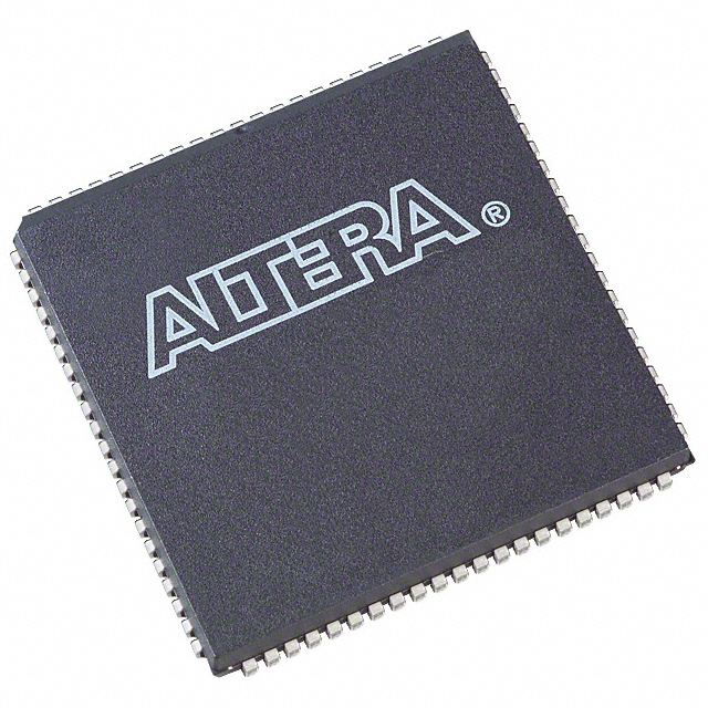
FLEX-10K® Field Programmable Gate Array (FPGA) IC 59 6144 576 84-LCC (J-Lead) |
|---|---|
| Quantity | 517 Available (as of October 8, 2026) |
| Product Category | Field Programmable Gate Array (FPGA) |
|---|---|
| Manufacturer | Intel |
| Manufacturing Status | Obsolete |
| Manufacturer Standard Lead Time | Contact Us |
| Datasheet |
Specifications & Environmental
| Device Package | 84-PLCC (29.31x29.31) | Grade | Commercial | Operating Temperature | 0°C – 70°C | ||
|---|---|---|---|---|---|---|---|
| Package / Case | 84-LCC (J-Lead) | Number of I/O | 59 | Voltage | 4.75 V - 5.25 V | ||
| Mounting Method | Surface Mount | RoHS Compliance | RoHS non-compliant | REACH Compliance | REACH Unaffected | ||
| Moisture Sensitivity Level | 3 (168 Hours) | Number of LABs/CLBs | 72 | Number of Logic Elements/Cells | 576 | ||
| Number of Gates | 31000 | ECCN | 3A991D | HTS Code | 8542.39.0001 | ||
| Qualification | N/A | Total RAM Bits | 6144 |
Overview of EPF10K10LC84-3 – FLEX-10K FPGA, 576 Logic Elements, ~6,144-bit Embedded RAM, 84-LCC (J‑Lead)
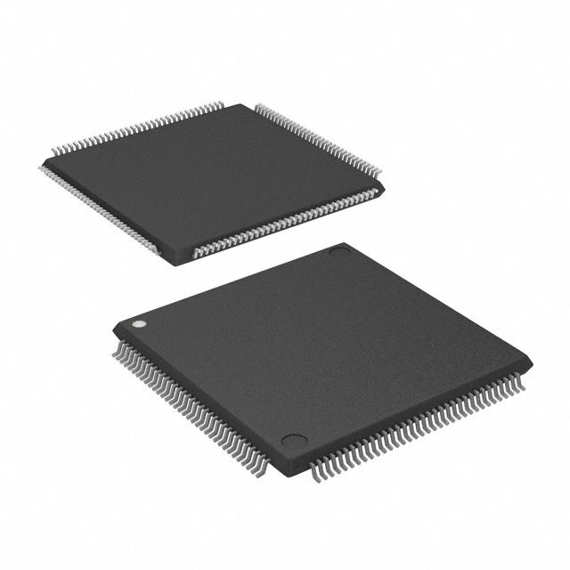
The EPF10K10LC84-3 is a FLEX-10K family Field Programmable Gate Array (FPGA) offered in an 84‑lead J‑lead LCC package. It combines a dedicated logic array and embedded memory resources to implement configurable logic, on‑chip RAM and system-level functions for commercial electronic designs.
Designed for applications that need moderate logic density and embedded RAM, this device delivers 576 logic elements, approximately 6,144 bits of embedded RAM, and a maximum system gate capacity of 31,000 in a surface‑mount 84‑lead package. Supply and thermal characteristics support 5.0 V operation and commercial temperature environments.
Key Features
- Logic Capacity — 576 logic elements and 72 LABs (logic array blocks) to implement mid-density programmable logic functions.
- On‑Chip Memory — Approximately 6,144 total RAM bits distributed across embedded array blocks (EABs) to support buffering, FIFOs and small embedded data structures.
- System Gates — Maximum system gates: 31,000, enabling integration of mixed logic and RAM resources for system-level functions.
- I/O and Packaging — 59 user I/O pins in a surface‑mount 84‑LCC (J‑Lead) package; supplier package reference 84‑PLCC (29.31×29.31 mm).
- Power and Voltage — Single supply operation at 4.75 V to 5.25 V aligns with 5.0 V systems and legacy I/O domains.
- Operating Range — Commercial grade: 0 °C to 70 °C.
- Built‑in Test and Reconfiguration — Includes IEEE 1149.1 JTAG boundary‑scan circuitry and supports in‑circuit reconfigurability via external configuration devices or the JTAG port.
- Architecture and Interconnect — FastTrack continuous routing, dedicated carry and cascade chains, tri‑state emulation, and multiple global clocks to support arithmetic, high‑fan‑in logic and clocking strategies.
- Low‑Power Standby — Typical standby consumption for most FLEX 10K devices is less than 0.5 mA (datasheet reference).
Typical Applications
- Embedded Control and System Integration — Implement control logic, glue logic and custom peripheral functions where on‑chip RAM and reconfigurability simplify board design.
- Memory and Buffering Functions — Use the device's embedded RAM blocks for small FIFOs, lookup tables and buffering in data paths.
- Peripheral and Bus Interfaces — Integrate custom bus logic or bridge functions; the FLEX 10K family provides PCI support in its documentation for system integration scenarios.
- Prototyping and OEM Products — Mid-density programmable fabric suitable for product variants and iterative hardware development within commercial temperature ranges.
Unique Advantages
- Balanced Logic and Memory — Combined 576 logic elements and embedded RAM enable implementation of both control logic and small data structures without external memory for many use cases.
- Reconfigurability — In‑circuit reconfiguration via external configuration devices or JTAG allows design updates and field changes without board swaps.
- Deterministic Routing and Arithmetic Support — FastTrack interconnect plus dedicated carry and cascade chains simplify high‑performance arithmetic and wide‑fan‑in functions when mapped by design tools.
- Package Flexibility — 84‑lead LCC surface‑mount package (supplier reference PLCC 29.31×29.31 mm) provides a compact footprint for space‑constrained commercial designs.
- Testability — Built‑in IEEE 1149.1 JTAG boundary‑scan reduces test complexity and supports board‑level diagnostics.
Why Choose EPF10K10LC84-3?
The EPF10K10LC84-3 positions itself as a practical, commercial‑grade FPGA for designs that require a moderate mix of programmable logic and embedded RAM in a compact surface‑mount package. Its combination of 576 logic elements, approximately 6,144 bits of on‑chip RAM, dedicated arithmetic chains and JTAG reconfiguration capability makes it suitable for system integration, interface bridging and prototype-to-production flows where 5.0 V operation and commercial temperature support are required.
Choosing this device delivers a reconfigurable, testable platform that reduces external component count and simplifies iterative design changes while leveraging the FLEX‑10K family architecture documented in the datasheet.
Request a quote or submit a pricing inquiry to receive availability and lead‑time information for EPF10K10LC84-3. Sales and distribution channels can provide part pricing, packaging details and order support.





















Date Founded: 1968
Headquarters: Santa Clara, California, USA
Employees: 130,000+
Revenue: $54.23 Billion
Certifications and Memberships: ISO9001:2015, ISO14001:2015, ISO17025:2017, ISO27001:2022, ISO45001:2018, ISO50001:2018


