
LCMXO3LF-4300E-6MG324C
| Part Description |
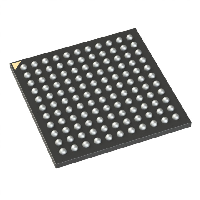
MachXO3 Field Programmable Gate Array (FPGA) IC 268 94208 4320 324-VFBGA |
|---|---|
| Quantity | 1,613 Available (as of October 8, 2026) |

| Product Category | Field Programmable Gate Array (FPGA) |
|---|---|
| Manufacturer | Lattice Semiconductor Corporation |
| Manufacturing Status | Active |
| Manufacturer Standard Lead Time | 20 Weeks |
| Datasheet |
Specifications & Environmental
| Device Package | 324-CSFBGA (10x10) | Grade | Commercial | Operating Temperature | 0°C – 85°C | ||
|---|---|---|---|---|---|---|---|
| Package / Case | 324-VFBGA | Number of I/O | 268 | Voltage | 1.14 V - 1.26 V | ||
| Mounting Method | Surface Mount | RoHS Compliance | ROHS3 Compliant | REACH Compliance | REACH Unaffected | ||
| Moisture Sensitivity Level | 3 (168 Hours) | Number of LABs/CLBs | 540 | Number of Logic Elements/Cells | 4320 | ||
| Number of Gates | N/A | ECCN | 3A991D | HTS Code | 8542.39.0001 | ||
| Qualification | N/A | Total RAM Bits | 94208 |
Overview of LCMXO3LF-4300E-6MG324C – MachXO3 Field Programmable Gate Array (FPGA) IC 268 94208 4320 324-VFBGA
The LCMXO3LF-4300E-6MG324C is a MachXO3 family Field Programmable Gate Array (FPGA) offered in a compact 324‑VFBGA package. It provides a balance of configurable logic, embedded memory and a high pin count for designs that require flexible I/O and reprogrammable on-chip logic in a commercial-grade device.
This device integrates 4,320 logic elements, approximately 0.094 Mbits of embedded RAM (94,208 bits), and 268 I/Os, with a 1.14 V to 1.26 V core supply range and an operating temperature of 0 °C to 85 °C. It is RoHS compliant and provided in a surface-mount 324-CSFBGA (10×10) package.
Key Features
- Configurable Logic 4,320 logic elements for implementing custom digital functions, state machines and glue logic.
- Embedded Memory Approximately 0.094 Mbits of on-chip RAM (94,208 bits) with support for multiple memory modes and FIFO configurations as part of the MachXO3 architecture.
- High I/O Count 268 I/Os with a flexible programmable I/O architecture suitable for varied interface requirements and source-synchronous I/O.
- Power and Voltage Core supply range of 1.14 V to 1.26 V supporting low-voltage operation; surface-mount package for compact board integration.
- System and Configuration Non-volatile, multi-time programmable configuration with on-chip configuration and reconfiguration features (TransFR reconfiguration and configuration options described in the MachXO3 family documentation).
- Embedded IP and Peripherals Hardened IP blocks including I²C and SPI cores, timer/counter and user flash memory (UFM) capabilities as described in the MachXO3 family data.
- Clocking and Timing On-chip oscillators and PLL-based clocking options for flexible on-chip clock distribution and system clocking.
- Package and Temperature 324‑VFBGA (supplier device package 324‑CSFBGA, 10×10), surface mount, commercial temperature range (0 °C to 85 °C).
- Regulatory RoHS compliant.
Typical Applications
- Interface and Glue Logic Ideal for implementing custom interface bridges, signal conditioning and board-level glue logic where flexible I/O and reprogrammable logic are required.
- Embedded System Control Suited for control, sequencing and peripheral management in commercial electronic products leveraging on-chip timers, I/O and embedded memory.
- Prototyping and Development Useful for designers building and iterating FPGA-based prototypes that need non‑volatile configuration and moderate logic density.
Unique Advantages
- Balanced Logic Density: 4,320 logic elements provide a practical capacity for mid-sized FPGA tasks without excessive board area.
- Ample I/O for Complex Interfaces: 268 programmable I/Os let you route multiple peripherals and high-pin-count interfaces directly to the device.
- Embedded Memory Resources: Approximately 0.094 Mbits of on-chip RAM supports local buffering, small FIFOs and state storage without external memory.
- Non‑volatile, Reprogrammable: Multi-time programmable configuration removes the need for an external configuration ROM while permitting design updates in the field.
- Compact, Surface-Mount Packaging: 324‑VFBGA / 324‑CSFBGA (10×10) keeps board footprint small for dense system designs.
- Commercial Temperature and RoHS Compliance: Commercial-grade operating range (0 °C to 85 °C) and RoHS compliance support standard product development and manufacturing flows.
Why Choose LCMXO3LF-4300E-6MG324C?
The LCMXO3LF-4300E-6MG324C is positioned for engineers who need a reprogrammable, non‑volatile FPGA with a balanced combination of logic resources, embedded RAM and a high I/O count in a compact package. Its MachXO3 family capabilities—on-chip memory, hardened peripheral IP and flexible clocking—make it suitable for mid-density logic tasks and board-level integration where a small footprint and reprogrammability matter.
This part is a fit for commercial electronic designs that require field-updatable logic, interface consolidation, and modest embedded memory without moving to larger, more complex FPGA families. The package, supply voltage range and documented MachXO3 architecture support straightforward integration into production systems and iterative development cycles.
Request a quote or submit a request for pricing and availability for the LCMXO3LF-4300E-6MG324C today.






















Date Founded: 1983
Headquarters: Hillsboro, Oregon, USA
Employees: 1,000+
Revenue: $627.7 Million
Certifications and Memberships: ISO9001:2015, ISO14001:2015, IATF16949:2016


