
LCMXO3LF-640E-5MG121I
| Part Description |
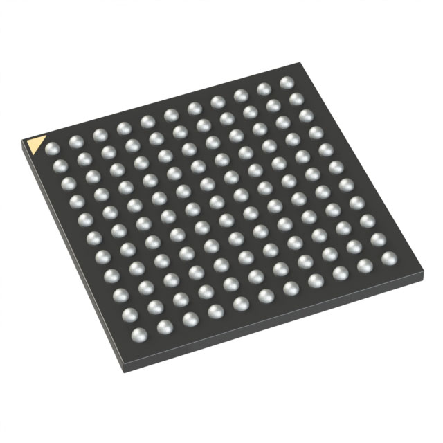
MachXO3 Field Programmable Gate Array (FPGA) IC 100 65536 640 121-VFBGA, CSPBGA |
|---|---|
| Quantity | 620 Available (as of June 15, 2026) |
| Product Category | Field Programmable Gate Array (FPGA) |
|---|---|
| Manufacturer | Lattice Semiconductor Corporation |
| Manufacturing Status | Active |
| Manufacturer Standard Lead Time | 20 Weeks |
| Datasheet |
Specifications & Environmental
| Device Package | 121-CSFBGA (6x6) | Grade | Industrial | Operating Temperature | -40°C – 100°C | ||
|---|---|---|---|---|---|---|---|
| Package / Case | 121-VFBGA, CSPBGA | Number of I/O | 100 | Voltage | 1.14 V - 1.26 V | ||
| Mounting Method | Surface Mount | RoHS Compliance | ROHS3 Compliant | REACH Compliance | REACH Unaffected | ||
| Moisture Sensitivity Level | 3 (168 Hours) | Number of LABs/CLBs | 80 | Number of Logic Elements/Cells | 640 | ||
| Number of Gates | N/A | ECCN | EAR99 | HTS Code | 8542.39.0001 | ||
| Qualification | N/A | Total RAM Bits | 65536 |
Overview of LCMXO3LF-640E-5MG121I – MachXO3 FPGA IC, 100 I/O, ~65.5Kbit RAM, 640 logic elements, 121‑VFBGA
The LCMXO3LF-640E-5MG121I is a MachXO3 family field programmable gate array (FPGA) offering non-volatile, multi-time programmable logic in a compact 121‑VFBGA (6×6) package. With 640 logic elements, approximately 65,536 bits of embedded RAM, and up to 100 I/O, this device targets board-level glue logic, I/O expansion and embedded peripheral control in industrial applications.
Designed for surface-mount assembly, the device supports a low core supply range (1.14 V to 1.26 V) and an industrial operating temperature window from -40 °C to 100 °C, enabling reliable operation across a wide set of embedded systems and control environments.
Key Features
- Logic Capacity — 640 logic elements for implementing custom combinational and sequential functions and board-level glue logic.
- Embedded Memory — Approximately 65,536 bits of on-chip RAM for small FIFOs, state storage, and buffering.
- I/O and Interface — Up to 100 I/O pins with programmable I/O cells and support for configurable I/O behavior as described in the MachXO3 family architecture.
- Non-volatile, Multi-time Programmable — MachXO3 family architecture provides non-volatile configuration and multi-time programmability for in-field updates.
- Hardened IP Blocks — Includes embedded hardened IP such as I²C, SPI and timer/counter cores for common peripheral and control tasks.
- Clocking and Timing — On-chip clocking features including PLLs and an on-chip oscillator for flexible clock generation and distribution.
- Power and Low-Power Modes — Standby mode and power-saving options available as part of the family feature set.
- Package and Mounting — 121‑VFBGA (CSPBGA 121‑CSFBGA, 6×6) surface-mount package optimized for compact board designs.
- Supply and Environmental — Core supply range 1.14 V to 1.26 V; industrial operating temperature range -40 °C to 100 °C; RoHS compliant.
Typical Applications
- Industrial control and automation — Use the device for sensor and peripheral interfacing and small control functions leveraging the 100 I/O and hardened I²C/SPI cores.
- Board-level glue logic — Consolidate discrete logic and bus bridging tasks into a single programmable device using 640 logic elements and on-chip RAM.
- Peripheral management — Implement SPI-based configuration, I²C sensor hubs, or timer-driven sequencing with the device’s embedded IP and timer/counter resources.
Unique Advantages
- Non-volatile programmability: Eliminates the need for external configuration memory by retaining configuration across power cycles.
- Compact package: 121‑VFBGA (6×6) CSPBGA reduces PCB footprint for space-constrained designs.
- Industrial temperature range: Rated from -40 °C to 100 °C for reliable operation in demanding environments.
- Integrated peripheral IP: Hardened I²C, SPI and timer/counter cores simplify common interface and timing tasks, reducing design effort and BOM.
- Flexible I/O and clocking: Programmable I/O cells, on-chip oscillator and PLLs provide adaptable timing and interface options without external components.
- RoHS compliant: Meets common environmental and manufacturing requirements for modern electronics production.
Why Choose LCMXO3LF-640E-5MG121I?
The LCMXO3LF-640E-5MG121I combines non-volatile MachXO3 family architecture, integrated peripheral IP, and a compact 121‑VFBGA package to deliver a practical, board-level FPGA solution for industrial and embedded designs. Its mix of 640 logic elements, ~65.5 Kbits of embedded RAM, and up to 100 I/O make it well suited for glue logic, interface bridging, and peripheral management where space and reliability matter.
For developers and procurement teams seeking a programmable, reconfigurable element with industrial temperature capability and built-in interface support, this MachXO3 device offers a scalable, application-friendly option backed by the family’s configuration, clocking and power management features.
Request a quote or submit an inquiry to receive pricing and availability for LCMXO3LF-640E-5MG121I. Our team can provide lead-time information and assist with volume requirements and qualification needs.


