
LCMXO3LF-6900C-5BG256I
| Part Description |
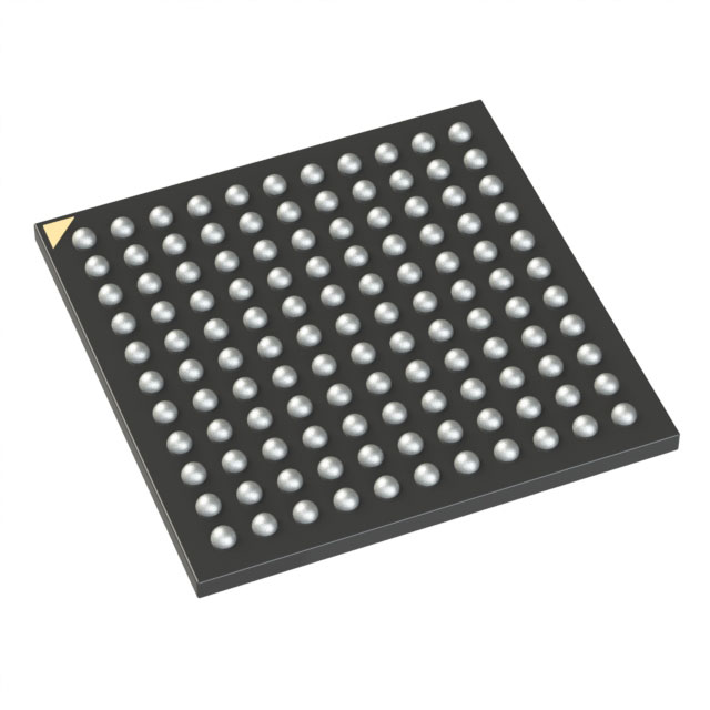
MachXO3 Field Programmable Gate Array (FPGA) IC 206 245760 6864 256-LFBGA |
|---|---|
| Quantity | 1,130 Available (as of October 7, 2026) |

| Product Category | Field Programmable Gate Array (FPGA) |
|---|---|
| Manufacturer | Lattice Semiconductor Corporation |
| Manufacturing Status | Active |
| Manufacturer Standard Lead Time | 20 Weeks |
| Datasheet |
Specifications & Environmental
| Device Package | 256-CABGA (14x14) | Grade | Industrial | Operating Temperature | -40°C – 100°C | ||
|---|---|---|---|---|---|---|---|
| Package / Case | 256-LFBGA | Number of I/O | 206 | Voltage | 2.375 V - 3.465 V | ||
| Mounting Method | Surface Mount | RoHS Compliance | ROHS3 Compliant | REACH Compliance | REACH Unaffected | ||
| Moisture Sensitivity Level | 3 (168 Hours) | Number of LABs/CLBs | 858 | Number of Logic Elements/Cells | 6864 | ||
| Number of Gates | N/A | ECCN | 3A991D | HTS Code | 8542.39.0001 | ||
| Qualification | N/A | Total RAM Bits | 245760 |
Overview of LCMXO3LF-6900C-5BG256I – MachXO3 Field Programmable Gate Array (FPGA) IC, 206 I/O, 245,760-bit RAM, 6,864 Logic Elements, 256-LFBGA
The LCMXO3LF-6900C-5BG256I is a MachXO3 family Field Programmable Gate Array (FPGA) IC designed for industrial applications. It combines 6,864 logic elements with 245,760 bits of embedded RAM and up to 206 I/Os in a 256-LFBGA package to support compact system integration and flexible hardware control.
Built on the MachXO3 architecture, the device provides non-volatile, multi-time programmable configuration and on-chip system resources such as programmable I/O, clocking and embedded IP building blocks, enabling reuse across control, bridging, and system-management functions in industrial designs.
Key Features
- Logic Capacity — 6,864 logic elements for glue logic, control functions and small to mid-density programmable tasks.
- Embedded Memory — 245,760 total RAM bits of on-chip memory supporting single, dual, pseudo-dual port and FIFO modes as described in the MachXO3 family datasheet.
- I/O and Packaging — Up to 206 I/Os in a 256-LFBGA (256-CABGA 14×14) surface-mount package to simplify board-level routing and high-density designs.
- Power and Temperature — Supports a supply range of 2.375 V to 3.465 V and an operating temperature range of −40 °C to 100 °C, rated for industrial-grade deployment.
- Non-volatile, Multi-time Programmable Configuration — On-device non-volatile configuration and TransFR reconfiguration support system-level flexibility described in the MachXO3 family documentation.
- Flexible On-chip Clocking — Integrated clocking features including PLLs and flexible clock distribution to support a variety of timing and synchronization needs.
- Programmable I/O and Source-Synchronous Support — Programmable I/O cells and pre-engineered source-synchronous I/O structures simplify interfacing to external devices and buses.
- Embedded Hardened IP — Family-level hardened functions such as I²C, SPI and timer/counter blocks provide off-the-shelf peripheral support as documented for MachXO3 devices.
- System and Power Management — On-chip oscillator, user flash memory (UFM), standby and power-saving options are provided at the family level to support low-power and system-management use cases.
- Standards and Testability — IEEE 1149.1-compliant boundary-scan support is included in family documentation for board-level testability and manufacturing diagnostics.
- Environmental Compliance — RoHS compliant.
Typical Applications
- Industrial Control — Industrial-grade thermal range (−40 °C to 100 °C) and robust I/O make the device suitable for factory automation controllers and machine-interface logic.
- Embedded System Glue Logic — 6,864 logic elements and 206 I/Os enable consolidation of glue logic, protocol adapters and control functions in embedded platforms.
- Interface Bridging and Timing — Programmable I/O cells and flexible on-chip clocking (PLLs and clock distribution) support board-level interface bridging and source-synchronous links.
- System Management and Peripherals — Embedded hardened IP (I²C, SPI, timers), UFM and standby modes help implement supervisory functions and peripheral control in constrained designs.
Unique Advantages
- Industrial operating range: Rated from −40 °C to 100 °C to meet extended-temperature deployments common in industrial applications.
- Integrated non-volatile configuration: Multi-time programmable, non-volatile configuration reduces the need for external configuration memory and simplifies system startup.
- Balanced integration: Combination of logic elements, embedded RAM and dedicated IP blocks reduces BOM count by consolidating multiple discrete functions into a single device.
- Flexible I/O and clocking: 206 I/Os plus source-synchronous and programmable clock resources simplify interfacing and timing-critical design tasks.
- Surface-mount, high-density package: 256-LFBGA (256-CABGA 14×14) provides a compact footprint for space-constrained boards while supporting high I/O count.
- Compliance and manufacturability: RoHS compliance and IEEE 1149.1 boundary-scan testability support regulatory and production needs.
Why Choose LCMXO3LF-6900C-5BG256I?
The LCMXO3LF-6900C-5BG256I delivers a pragmatic balance of logic capacity, embedded memory and a high I/O count in a compact 256-LFBGA package targeted at industrial and embedded designs. Family-level features such as non-volatile multi-time programmable configuration, programmable I/O, flexible clocking and hardened peripheral IP enable rapid integration of control, interface and system-management functions without relying on numerous discrete components.
This device is well suited for engineers seeking a scalable, industrial-grade FPGA solution with documented MachXO3 family resources for configuration, memory modes, clocking and embedded peripherals—helping reduce board complexity and long-term maintenance in production systems.
Request a quote or submit an RFQ to receive pricing and availability information for the LCMXO3LF-6900C-5BG256I.























Date Founded: 1983
Headquarters: Hillsboro, Oregon, USA
Employees: 1,000+
Revenue: $627.7 Million
Certifications and Memberships: ISO9001:2015, ISO14001:2015, IATF16949:2016


