
M1A3P1000-2FGG484
| Part Description |
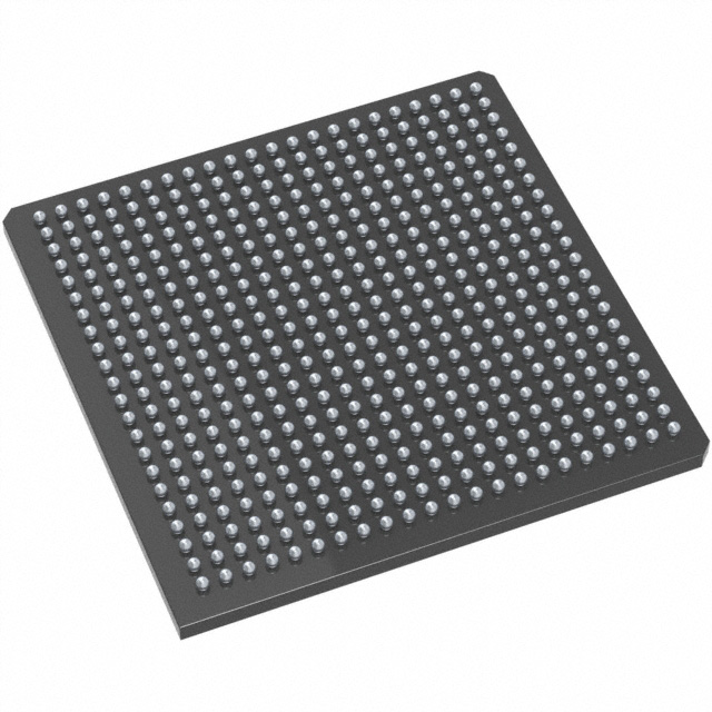
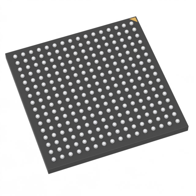
ProASIC3 Field Programmable Gate Array (FPGA) IC 300 147456 484-BGA |
|---|---|
| Quantity | 613 Available (as of October 8, 2026) |
| Product Category | Field Programmable Gate Array (FPGA) |
|---|---|
| Manufacturer | Microchip Technology |
| Manufacturing Status | Active |
| Manufacturer Standard Lead Time | 18 Weeks |
| Datasheet |
Specifications & Environmental
| Device Package | 484-FPBGA (23x23) | Grade | Commercial | Operating Temperature | 0°C – 85°C | ||
|---|---|---|---|---|---|---|---|
| Package / Case | 484-BGA | Number of I/O | 300 | Voltage | 1.425 V - 1.575 V | ||
| Mounting Method | Surface Mount | RoHS Compliance | ROHS3 Compliant | REACH Compliance | REACH Unaffected | ||
| Moisture Sensitivity Level | 3 (168 Hours) | Number of LABs/CLBs | 24576 | Number of Logic Elements/Cells | 24576 | ||
| Number of Gates | 1000000 | ECCN | 3A991D | HTS Code | 8542.39.0001 | ||
| Qualification | N/A | Total RAM Bits | 147456 |
Overview of M1A3P1000-2FGG484 – ProASIC3 Field Programmable Gate Array IC, 300 I/Os, 147,456-bit RAM, 484-BGA
The M1A3P1000-2FGG484 is a ProASIC3 family FPGA offering a high-density, flash-based reprogrammable fabric in a 484-ball BGA package. Designed for applications that require a balance of logic capacity, on-chip memory, and extensive I/O, this device targets portable and high-volume consumer designs as well as low-power embedded systems.
This surface-mount device integrates approximately 24,576 logic elements and 147,456 bits of embedded memory, with up to 300 user I/Os, delivering a compact single-chip solution for instant-on, secure, and power-conscious designs.
Key Features
- Core Logic Approximately 24,576 logic elements (logic element cells) supporting a system gate equivalent of about 1,000,000 gates for mid-range FPGA integration.
- Embedded Memory Total on-chip RAM of 147,456 bits — approximately 0.147 Mbits of embedded memory for SRAM and FIFO structures.
- I/O Capacity & Flexibility Up to 300 user I/Os with support for mixed-voltage operation (1.5V, 1.8V, 2.5V, 3.3V) and bank-selectable I/O voltages to interface with a wide range of peripherals and subsystems.
- Programming & Security (Series Features) Flash-based reprogrammable technology with in-system programming via JTAG and on-chip AES decryption for secured configuration and content protection.
- Power Core supply range specified at 1.425 V to 1.575 V, enabling low-voltage operation consistent with 1.5V core architectures for reduced power consumption.
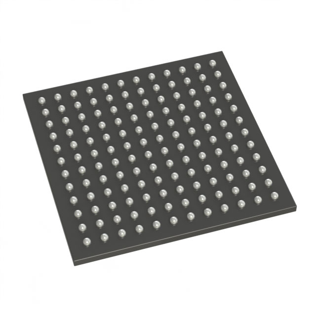
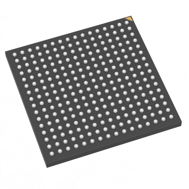
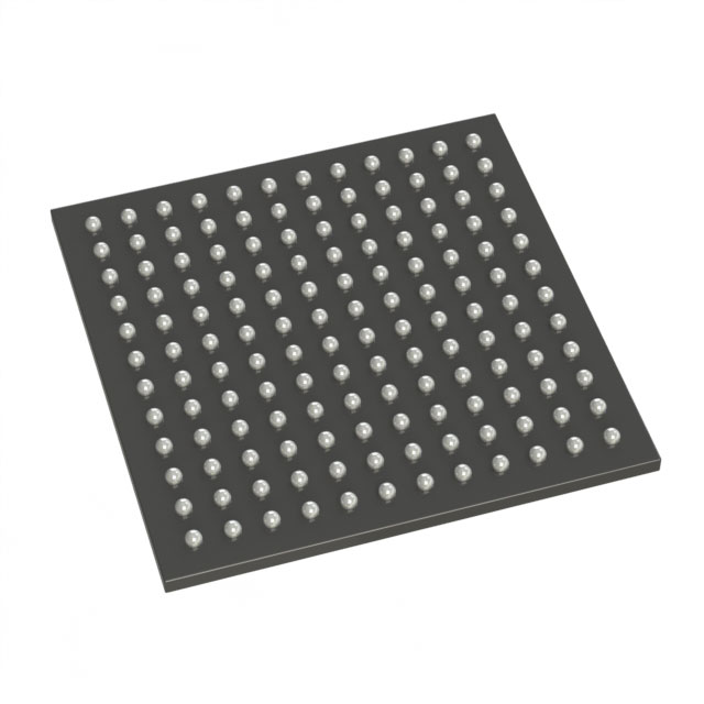
- Package & Mounting 484-FPBGA (23 × 23) package, surface-mount mounting type, optimized for compact PCB layouts and high-density board integration.
- Operating Environment & Compliance Commercial-grade operating temperature from 0 °C to 85 °C and RoHS-compliant construction.
Typical Applications
- Portable Consumer Electronics Use for instant-on control, user interfaces, and peripheral aggregation where low power and compact packaging are important.
- Battery-Powered Systems Suitable for designs that need flash-based nonvolatility and low core-voltage operation to extend battery life.
- Secure Embedded Solutions Applies to products requiring in-system programming with hardware AES decryption and FlashLock-style protection to secure bitstreams.
- High-Density I/O Control Ideal for applications that require many external interfaces—sensor hubs, display controllers, or I/O concentrators—leveraging up to 300 user I/Os.
Unique Advantages
- Reprogrammable Flash-Based Design: Retains programmed configuration when powered off, enabling instant-on behavior and flexible field updates without external memory.
- High I/O Count in a Compact Package: 300 available I/Os in a 484-BGA footprint helps reduce board-level complexity and connector count for dense system designs.
- Low-Voltage Core Operation: Specified core supply of 1.425 V to 1.575 V supports energy-efficient designs and compatibility with 1.5V-only systems.
- Integrated Security & ISP: On-chip AES decryption and secure programming workflows enable protected configuration and secure in-field updates.
- Commercial Temperature Range & RoHS Compliance: Commercial-grade temperature rating (0 °C to 85 °C) and RoHS compliance streamline deployment in consumer and commercial products.
Why Choose M1A3P1000-2FGG484?
The M1A3P1000-2FGG484 combines substantial logic capacity and embedded memory with a high I/O count in a compact 484-BGA package, offering a practical balance of performance, integration, and power efficiency for commercial embedded designs. Its flash-based reprogrammability and on-chip security features support flexible development cycles and secure deployment.
Choose this ProASIC3 FPGA when your design requires a single-chip, reprogrammable solution with broad I/O capability, low-voltage core operation, and RoHS compliance—well suited for consumer, portable, and other commercial applications where board space and power matter.
Request a quote or submit an inquiry to receive pricing and availability for the M1A3P1000-2FGG484 and to discuss how it can fit your next design.





















Date Founded: 1989
Headquarters: Chandler, Arizona, USA
Employees: 22,000+
Revenue: $8.349 Billion
Certifications and Memberships: ISO9001:2015, IATF16949:2016, AS 9100D




