
M1A3P1000-2FGG256I
| Part Description |
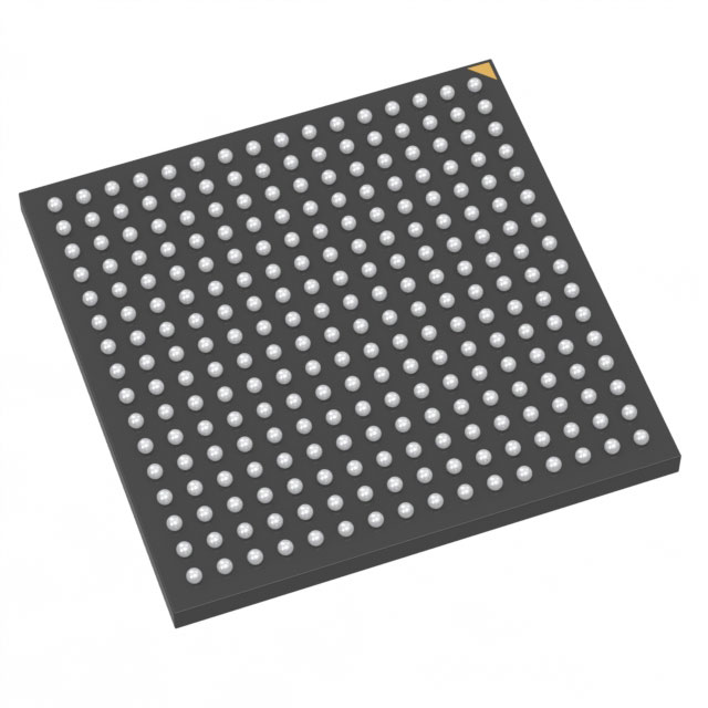
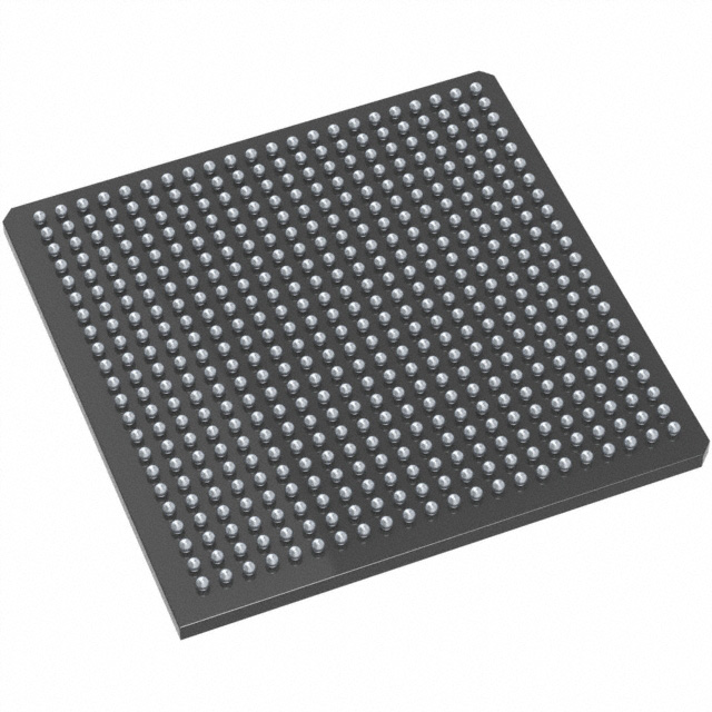
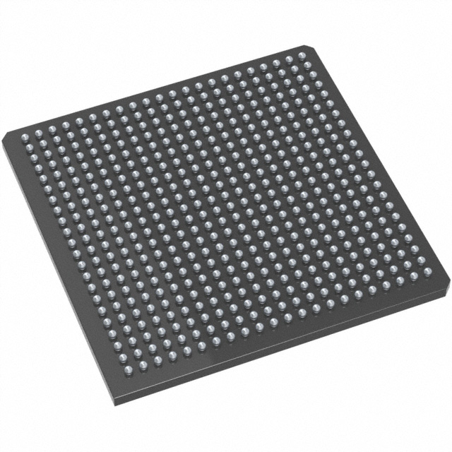
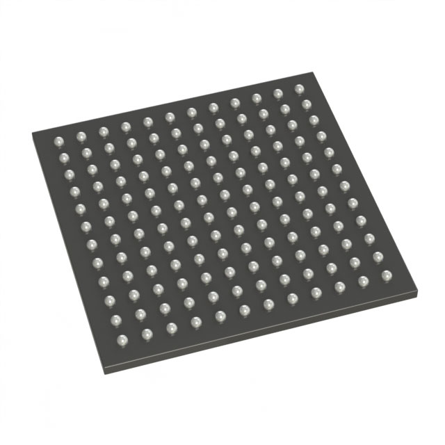
ProASIC3 Field Programmable Gate Array (FPGA) IC 177 147456 256-LBGA |
|---|---|
| Quantity | 1,323 Available (as of October 8, 2026) |
| Product Category | Field Programmable Gate Array (FPGA) |
|---|---|
| Manufacturer | Microchip Technology |
| Manufacturing Status | Active |
| Manufacturer Standard Lead Time | 18 Weeks |
| Datasheet |
Specifications & Environmental
| Device Package | 256-FPBGA (17x17) | Grade | Industrial | Operating Temperature | -40°C – 100°C | ||
|---|---|---|---|---|---|---|---|
| Package / Case | 256-LBGA | Number of I/O | 177 | Voltage | 1.425 V - 1.575 V | ||
| Mounting Method | Surface Mount | RoHS Compliance | ROHS3 Compliant | REACH Compliance | REACH Unaffected | ||
| Moisture Sensitivity Level | 3 (168 Hours) | Number of LABs/CLBs | 24576 | Number of Logic Elements/Cells | 24576 | ||
| Number of Gates | 1000000 | ECCN | 3A991D | HTS Code | 8542.39.0001 | ||
| Qualification | N/A | Total RAM Bits | 147456 |
Overview of M1A3P1000-2FGG256I – ProASIC3 Field Programmable Gate Array, 177 I/Os, 256‑LBGA
The M1A3P1000-2FGG256I is a ProASIC3 family Field Programmable Gate Array (FPGA) in a 256‑LBGA package designed for industrial applications. It combines reprogrammable, nonvolatile flash-based FPGA architecture with a substantial logic capacity and on‑chip RAM to support control, interface, and system‑level integration tasks.
This device is suited for designs requiring moderate logic density and robust operating conditions, offering 24,576 logic elements, approximately 0.147 Mbits of embedded memory, and 177 user I/Os in a surface‑mount, 256‑FPBGA (17×17) package.
Key Features
- Core Logic — 24,576 logic elements (reported as Number Of Logic Elements Cells) and 1,000,000 gates provide substantial programmable logic capacity for mid‑density designs.
- Embedded Memory — Total on‑chip RAM of 147,456 bits (approximately 0.147 Mbits) for FIFOs, buffers, and small data stores.
- I/O Count — 177 user I/Os to support complex interfacing and multi‑signal connectivity on a single device.
- Nonvolatile, Flash‑Based Configuration — ProASIC3 family documentation describes flash-based, reprogrammable, nonvolatile devices that retain design configuration when powered off.
- Voltage Supply — Core supply range specified at 1.425 V to 1.575 V, enabling designs that target a 1.5 V core domain.
- Package & Mounting — Surface‑mount 256‑LBGA; supplier device package listed as 256‑FPBGA (17×17) for compact board integration.
- Industrial Temperature Grade — Rated for operation from −40 °C to 100 °C to meet industrial environment requirements.
- RoHS Compliant — Device meets RoHS environmental requirements as specified in the product data.
Typical Applications
- Industrial Control and Automation — Implements custom logic, protocol conversion, and I/O aggregation in industrial systems that require extended temperature operation.
- Communications and Networking — Provides programmable interface and protocol handling with 177 I/Os for medium‑density port aggregation and signal routing.
- Instrumentation and Test Equipment — Enables flexible signal processing, timing control, and data buffering using embedded RAM and ample logic resources.
- Consumer and Portable Systems — As described for the ProASIC3 family, suitable for portable and battery‑backed markets where nonvolatile, instant‑on behavior is beneficial.
Unique Advantages
- High Logic Density — 24,576 logic elements and 1,000,000 gates deliver the capacity to consolidate multiple functions into a single programmable device, reducing BOM and interconnect complexity.
- Nonvolatile Configuration — Flash‑based reprogrammable logic retains the programmed design after power‑off, simplifying deployment in systems that require instant availability on power‑up.
- Broad I/O Capability — 177 user I/Os enable diverse peripheral interfacing and multiple banked I/O arrangements on a single package.
- Industrial Reliability — Operation across −40 °C to 100 °C and surface‑mount 256‑LBGA packaging support robust deployment in demanding environments.
- Compact Package — 256‑FPBGA (17×17) footprint balances board area and I/O count for space‑constrained designs.
- Compliance and Assembly — RoHS compliance aids regulatory and manufacturing readiness for many markets.
Why Choose M1A3P1000-2FGG256I?
The M1A3P1000-2FGG256I is positioned for engineers who need a reprogrammable, nonvolatile FPGA with mid‑range logic and memory capacity, a high I/O count, and industrial temperature operation. Its combination of 24,576 logic elements, approximately 0.147 Mbits of embedded RAM, and 177 I/Os in a compact 256‑LBGA package makes it suitable for consolidating control, interface, and buffering functions into a single device.
This device offers long‑term value for product lines that require field reprogrammability, reduced component count, and reliable operation across industrial temperature ranges, while maintaining the flexibility of FPGA‑based design updates.
Request a quote or submit an inquiry for pricing and availability of M1A3P1000-2FGG256I to evaluate integration into your next design.





















Date Founded: 1989
Headquarters: Chandler, Arizona, USA
Employees: 22,000+
Revenue: $8.349 Billion
Certifications and Memberships: ISO9001:2015, IATF16949:2016, AS 9100D




