
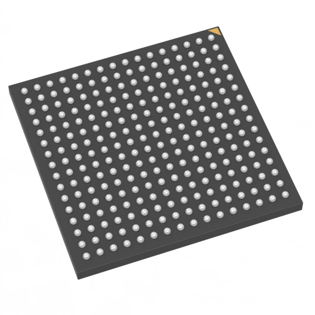
M1A3P1000-2FGG256
| Part Description |
ProASIC3 Field Programmable Gate Array (FPGA) IC 177 147456 256-LBGA |
|---|---|
| Quantity | 1,603 Available (as of June 15, 2026) |
| Product Category | Field Programmable Gate Array (FPGA) |
|---|---|
| Manufacturer | Microchip Technology |
| Manufacturing Status | Active |
| Manufacturer Standard Lead Time | 18 Weeks |
| Datasheet |
Specifications & Environmental
| Device Package | 256-FPBGA (17x17) | Grade | Commercial | Operating Temperature | 0°C – 85°C | ||
|---|---|---|---|---|---|---|---|
| Package / Case | 256-LBGA | Number of I/O | 177 | Voltage | 1.425 V - 1.575 V | ||
| Mounting Method | Surface Mount | RoHS Compliance | ROHS3 Compliant | REACH Compliance | REACH Unaffected | ||
| Moisture Sensitivity Level | 3 (168 Hours) | Number of LABs/CLBs | 24576 | Number of Logic Elements/Cells | 24576 | ||
| Number of Gates | 1000000 | ECCN | 3A991D | HTS Code | 8542.39.0001 | ||
| Qualification | N/A | Total RAM Bits | 147456 |
Overview of M1A3P1000-2FGG256 – ProASIC3 Field Programmable Gate Array (FPGA) IC 177 I/Os, 147,456 bits RAM, 256-LBGA
The M1A3P1000-2FGG256 is a ProASIC3 flash-based FPGA from Microchip Technology, offering a nonvolatile, reprogrammable single-chip solution. It combines a high-logic capacity fabric with embedded memory and flexible I/O to address cost-sensitive, space-constrained designs in consumer, portable, and other commercial markets.
Designed for applications that require instant-on behavior, hardware security and low power operation, this device provides a balance of integration and configurability for fast time-to-market and ASIC/ASSP replacement scenarios.
Key Features
- Logic Capacity — 24,576 logic elements (equivalent macrocells) and approximately 1,000,000 system gates for mid-density logic integration.
- Embedded Memory — 147,456 bits of on-chip RAM (approximately 0.147 Mbits) to support data buffering, FIFOs and small working sets.
- I/O and Mixed-Voltage Support — 177 user I/Os with bank-selectable voltages; series supports 1.5V, 1.8V, 2.5V and 3.3V single-ended standards for mixed-voltage designs.
- Reprogrammable Flash Technology — Flash-based CMOS process with instant-on capability and retained configuration when power is removed.
- Security and In-System Programming — On-chip 128-bit AES decryption for JTAG-based in-system programming and FlashLock protection for securing FPGA contents.
- Clocking and Timing — High-performance routing and clock hierarchy with configurable Clock Conditioning Circuit blocks and integrated PLL options (series feature).
- Power and Supply — Core supply range of 1.425 V to 1.575 V, optimized for low-power single-core operation consistent with the ProASIC 3 nano family.
- Package and Temperature — 256-LBGA surface-mount package (256-FPBGA, 17×17) and commercial operating temperature range of 0 °C to 85 °C.
- RoHS Compliant — Device meets RoHS environmental requirements.
Typical Applications
- Consumer & Portable Electronics — Instant-on, low-power operation and a compact 256-LBGA package suit portable and battery-backed devices requiring flexible logic and I/O.
- ASIC/ASSP Replacement — Reprogrammable flash architecture and mid-range logic density enable iterative development and cost-effective replacements for fixed-function ASICs or ASSPs.
- Secure In-System Updates — On-chip AES decryption and FlashLock support secure configuration updates and protected field upgrades in commercial products.
Unique Advantages
- Nonvolatile, Instant-On Design: Flash-based configuration retains programmed logic when powered off and supports instant-on system behavior.
- Balanced Integration: 24,576 logic elements combined with approximately 0.147 Mbits of embedded RAM reduces external component count for compact designs.
- Flexible Mixed-Voltage I/O: Bank-selectable I/O voltages and a large count of user I/Os (177) simplify interfacing with multiple voltage domains and peripherals.
- Built-in Security and ISP: 128-bit AES in-system decryption and FlashLock provide hardware-level protection for configuration images and field programming.
- Low-Power Core Supply: Operates from a 1.425 V to 1.575 V core supply to support energy-conscious commercial applications.
- Commercial Temperature and RoHS Compliance: Specified 0 °C to 85 °C operation and RoHS compliance for mainstream commercial product deployments.
Why Choose M1A3P1000-2FGG256?
The M1A3P1000-2FGG256 positions itself as a mid-density, flash-configured FPGA that delivers reprogrammable logic, embedded memory and a high I/O count in a compact 256-LBGA package. It is well suited for commercial projects that demand secure in-field programmability, reduced BOM and fast development cycles.
Backed by Microchip’s ProASIC3 family architecture and supporting documentation, this device is appropriate for designers seeking a nonvolatile FPGA platform with integrated security, mixed-voltage interfacing and a focus on low-power operation.
Request a quote or submit an inquiry to obtain pricing, availability and integration support for the M1A3P1000-2FGG256.


Date Founded: 1989
Headquarters: Chandler, Arizona, USA
Employees: 22,000+
Revenue: $8.349 Billion
Certifications and Memberships: ISO9001:2015, IATF16949:2016, AS 9100D


