
M1A3P1000-2FGG144I
| Part Description |
ProASIC3 Field Programmable Gate Array (FPGA) IC 97 147456 144-LBGA |
|---|---|
| Quantity | 904 Available (as of June 14, 2026) |

| Product Category | Field Programmable Gate Array (FPGA) |
|---|---|
| Manufacturer | Microchip Technology |
| Manufacturing Status | Active |
| Manufacturer Standard Lead Time | 18 Weeks |
| Datasheet |
Specifications & Environmental
| Device Package | 144-FPBGA (13x13) | Grade | Industrial | Operating Temperature | -40°C – 100°C | ||
|---|---|---|---|---|---|---|---|
| Package / Case | 144-LBGA | Number of I/O | 97 | Voltage | 1.425 V - 1.575 V | ||
| Mounting Method | Surface Mount | RoHS Compliance | ROHS3 Compliant | REACH Compliance | REACH Unaffected | ||
| Moisture Sensitivity Level | 3 (168 Hours) | Number of LABs/CLBs | 24576 | Number of Logic Elements/Cells | 24576 | ||
| Number of Gates | 1000000 | ECCN | 3A991D | HTS Code | 8542.39.0001 | ||
| Qualification | N/A | Total RAM Bits | 147456 |
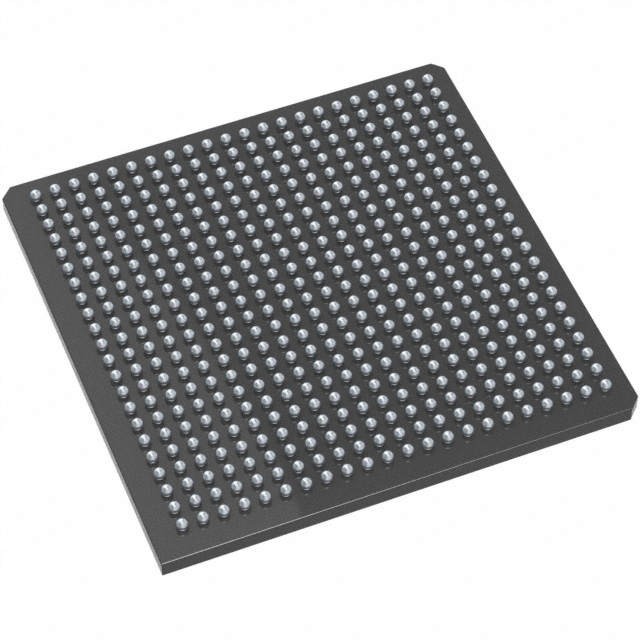
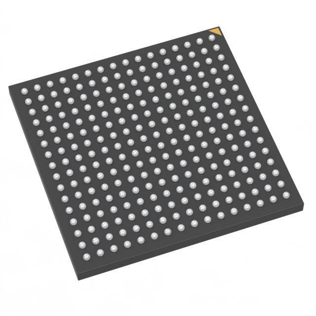
Overview of M1A3P1000-2FGG144I – ProASIC3 Flash FPGA, 97 I/Os, 24,576 logic elements, 144-LBGA
The M1A3P1000-2FGG144I is a ProASIC3 flash-based Field Programmable Gate Array (FPGA) from Microchip Technology. It delivers a nonvolatile, instant-on FPGA solution with a high logic density and abundant I/O suited for industrial embedded applications.
Designed for applications that require integration, secure in-system updates, and deterministic I/O, this device combines 24,576 logic elements, roughly 1,000,000 system gates and approximately 0.147 Mbits of embedded memory with a 144-LBGA package and industrial temperature range.
Key Features
- Core & Logic: 24,576 logic elements and 1,000,000 system gates provide substantial combinational and sequential capability for mid-to-high density designs.
- Embedded Memory: Total on-chip RAM of 147,456 bits (approximately 0.147 Mbits) for data storage, FIFOs and buffering inside the fabric.
- I/O & Interface Flexibility: 97 user I/Os accommodate diverse external interfaces and peripherals; the family supports mixed-voltage I/O operation per series features.
- Nonvolatile Flash Technology: Flash-based configuration provides instant-on operation and retains the programmed design when powered off.
- Security & In-System Programming: Series-level features include on-chip AES (128-bit) decryption for secure JTAG ISP and FlashLock to protect FPGA contents.
- Power & Voltage: Core supply range of 1.425 V to 1.575 V enables low-power operation consistent with 1.5 V core architectures; device is surface-mount.
- Package & Mechanical: 144-LBGA package; supplier device package noted as 144-FPBGA (13×13) to support compact PCB layouts.
- Industrial Temperature Rating: Rated for operation from −40 °C to 100 °C, suitable for industrial environments.
- RoHS Compliant: Meets RoHS requirements for environmental compliance.
Typical Applications
- Industrial Control: Deterministic I/O and nonvolatile configuration make this FPGA suitable for PLCs, motor controllers and factory automation modules.
- Embedded Systems: Use for edge compute, protocol bridging and custom logic acceleration where instant-on behavior and retained configuration are required.
- Secure Field Upgrades: Flash-based ISP with AES decryption supports secure in-field firmware updates and protected design IP.
- Sensor and I/O Aggregation: High I/O count and on-chip memory enable aggregation, buffering and preprocessing of sensor data in industrial instrumentation.
Unique Advantages
- Nonvolatile, Instant-On Operation: Flash configuration removes the need for external configuration memory and enables immediate startup with the programmed design.
- Secure In-System Programming: On-chip AES-based ISP and FlashLock protect design integrity during field updates and manufacturing programming.
- High Logic Density: 24,576 logic elements and 1,000,000 gates provide capacity for complex control, signal processing and glue-logic integration.
- Industrial Reliability: Specified for −40 °C to 100 °C operation, supporting deployment in demanding industrial environments.
- Flexible I/O Count: 97 user I/Os offer broad interfacing capability to sensors, actuators and peripherals without external multiplexing.
- Compact Surface-Mount Package: 144-LBGA / 144-FPBGA (13×13) enables dense board designs while maintaining thermal and mechanical robustness.
Why Choose M1A3P1000-2FGG144I?
The M1A3P1000-2FGG144I positions itself as an industrial-grade, flash-based FPGA delivering high logic capacity, substantial on-chip memory and a robust I/O complement in a compact 144-LBGA package. Its nonvolatile configuration and secure ISP capability are particularly valuable for designs that require retained programming, secure field updates and deterministic startup behavior.
This device is a strong fit for engineers building industrial embedded systems, automation equipment, and secure edge modules who need a single-chip, low-voltage FPGA solution backed by Microchip Technology.
Request a quote or submit an inquiry to obtain pricing and availability for the M1A3P1000-2FGG144I.


Date Founded: 1989
Headquarters: Chandler, Arizona, USA
Employees: 22,000+
Revenue: $8.349 Billion
Certifications and Memberships: ISO9001:2015, IATF16949:2016, AS 9100D


