
M1A3P1000-2FG256I
| Part Description |
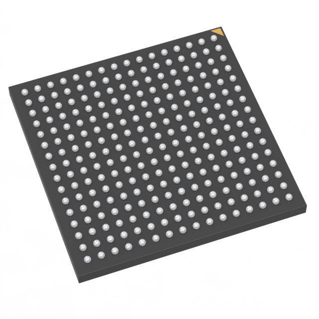
ProASIC3 Field Programmable Gate Array (FPGA) IC 177 147456 256-LBGA |
|---|---|
| Quantity | 240 Available (as of June 18, 2026) |
| Product Category | Field Programmable Gate Array (FPGA) |
|---|---|
| Manufacturer | Microchip Technology |
| Manufacturing Status | Active |
| Manufacturer Standard Lead Time | 18 Weeks |
| Datasheet |
Specifications & Environmental
| Device Package | 256-FPBGA (17x17) | Grade | Industrial | Operating Temperature | -40°C – 100°C | ||
|---|---|---|---|---|---|---|---|
| Package / Case | 256-LBGA | Number of I/O | 177 | Voltage | 1.425 V - 1.575 V | ||
| Mounting Method | Surface Mount | RoHS Compliance | RoHS non-compliant | REACH Compliance | REACH Unaffected | ||
| Moisture Sensitivity Level | 3 (168 Hours) | Number of LABs/CLBs | 24576 | Number of Logic Elements/Cells | 24576 | ||
| Number of Gates | 1000000 | ECCN | 3A991D | HTS Code | 8542.39.0001 | ||
| Qualification | N/A | Total RAM Bits | 147456 |
Overview of M1A3P1000-2FG256I – ProASIC3 Field Programmable Gate Array (FPGA) IC 177 147456 256-LBGA
The M1A3P1000-2FG256I is a ProASIC3 family Field Programmable Gate Array (FPGA) offered in a 256-LBGA package. It provides a flash-based FPGA architecture with a high logic element count, ample embedded RAM and a broad I/O complement suitable for industrial embedded designs.
Targeted at industrial applications, this device combines 24,576 logic elements, approximately 147,456 bits of on-chip RAM, and 177 I/O pins in a surface-mount 256-FPBGA (17×17) package, operating across a 1.425 V–1.575 V core supply and an ambient range of −40 °C to 100 °C.
Key Features
- Logic Density 24,576 logic elements (cells) delivering up to 1,000,000 gates of programmable logic for medium-density FPGA designs.
- Embedded Memory 147,456 bits of total on-chip RAM (approximately 0.147 Mbits) for temporary storage, buffering and scratchpad memory.
- I/O Capacity 177 general-purpose I/O pins to support multiple interfaces and external peripherals.
- Flash-Based Architecture Part of the ProASIC3 family of low-power flash FPGAs; family documentation references Flash*Freeze technology for low-power retention modes.
- Power Supply Core operating voltage range of 1.425 V to 1.575 V to match system power domains precisely.
- Package and Mounting Surface-mount 256-LBGA package; supplier device package listed as 256-FPBGA (17×17) for compact board-level integration.
- Industrial Temperature Qualified for operation from −40 °C to 100 °C to meet demanding environmental conditions.
- Compliance RoHS compliant.
Typical Applications
- Industrial Control Implement control logic, protocol bridging and sequencing functions using the device’s abundant logic elements and I/O resources.
- Communications Equipment Use the FPGA’s programmable fabric and on-chip RAM for custom packet processing, interface adaptation and buffering.
- Test & Measurement Create deterministic timing engines, data acquisition front-ends and signal routing logic leveraging the device’s logic density and IO count.
- Embedded Processing and Peripherals Integrate peripheral controllers, glue logic and customized accelerators where compact package size and industrial temperature range are required.
Unique Advantages
- High Logic Capacity: 24,576 logic elements and 1,000,000 gates provide the resources needed for complex, integrated designs without external glue logic.
- Significant On‑Chip Memory: Approximately 147,456 bits of embedded RAM supports buffering and local storage, reducing external memory dependencies.
- Large I/O Count: 177 I/O pins enable multiple parallel interfaces and flexible board-level routing options.
- Compact, Surface‑Mount Package: 256-LBGA / 256-FPBGA (17×17) package balances board density with thermal and routing considerations.
- Industrial Temperature Range: Rated for −40 °C to 100 °C operation to support deployments in harsh environments.
- Flash-Based, Low-Power Family Features: ProASIC3 family characteristics include flash-based configuration and documented Flash*Freeze technology for low-power retention modes.
- Regulatory Compliance: RoHS compliant for streamlined environmental qualification.
Why Choose M1A3P1000-2FG256I?
The M1A3P1000-2FG256I positions itself as a robust industrial-grade FPGA option that brings together substantial logic density, embedded memory and a large I/O count in a compact 256-LBGA footprint. Its specified operating voltage and wide temperature range make it suitable for applications that require stable, long-term operation in industrial environments.
Designers seeking a flash-based programmable device with on-chip RAM and extensive I/O capability will find this part appropriate for medium-complexity FPGA functions where board space, thermal profile and environmental tolerance are important. RoHS compliance and the ProASIC3 family feature set support integration into regulated, production-grade systems.
Request a quote or submit an inquiry for M1A3P1000-2FG256I to discuss availability, pricing and lead time for your design needs.


Date Founded: 1989
Headquarters: Chandler, Arizona, USA
Employees: 22,000+
Revenue: $8.349 Billion
Certifications and Memberships: ISO9001:2015, IATF16949:2016, AS 9100D


