
M1A3P1000-2FG256
| Part Description |
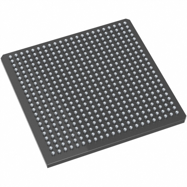
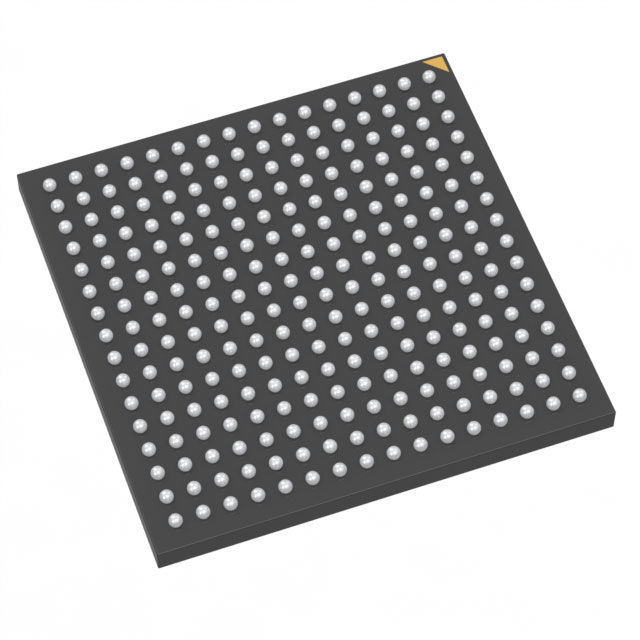
ProASIC3 Field Programmable Gate Array (FPGA) IC 177 147456 256-LBGA |
|---|---|
| Quantity | 997 Available (as of June 15, 2026) |

| Product Category | Field Programmable Gate Array (FPGA) |
|---|---|
| Manufacturer | Microchip Technology |
| Manufacturing Status | Active |
| Manufacturer Standard Lead Time | 18 Weeks |
| Datasheet |
Specifications & Environmental
| Device Package | 256-FPBGA (17x17) | Grade | Commercial | Operating Temperature | 0°C – 85°C | ||
|---|---|---|---|---|---|---|---|
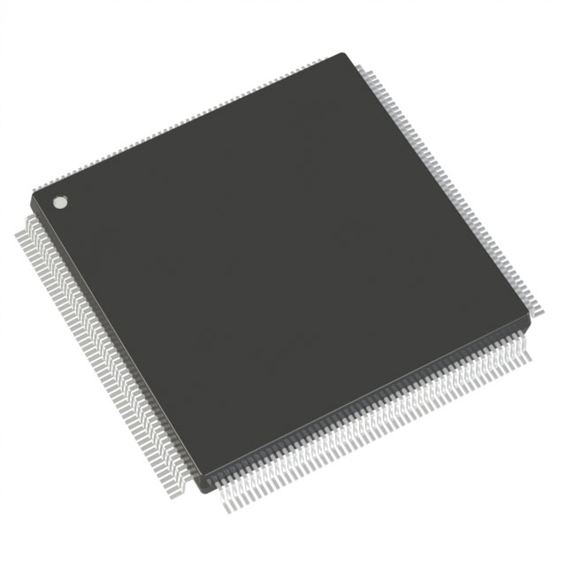
| Package / Case | 256-LBGA | Number of I/O | 177 | Voltage | 1.425 V - 1.575 V | ||
| Mounting Method | Surface Mount | RoHS Compliance | RoHS non-compliant | REACH Compliance | REACH Unaffected | ||
| Moisture Sensitivity Level | 3 (168 Hours) | Number of LABs/CLBs | 24576 | Number of Logic Elements/Cells | 24576 | ||
| Number of Gates | 1000000 | ECCN | 3A991D | HTS Code | 8542.39.0001 | ||
| Qualification | N/A | Total RAM Bits | 147456 |
Overview of M1A3P1000-2FG256 – ProASIC3 Field Programmable Gate Array, 256-LBGA
The M1A3P1000-2FG256 is a ProASIC3 flash-based Field Programmable Gate Array (FPGA) from Microchip Technology. It provides a mid-range programmable fabric with 24,576 logic elements and on-chip flash memory architecture suitable for embedded control, glue logic and interface functions.
Designed for surface-mount assembly in a 256-LBGA package, this device combines a defined core voltage range and commercial temperature rating to serve applications that require a balance of logic capacity, I/O density and compact packaging.
Key Features
- Core / Logic Capacity Approximately 24,576 logic elements (24576 logic elements) and an internal equivalent of 1,000,000 gates for mid-range programmable logic implementations.
- Embedded Memory Total on-chip RAM of 147,456 bits — approximately 0.147 Mbits of embedded memory for local buffering and small data structures.
- I/O Density 177 user I/O pins to support multiple signals, interfaces and board-level interconnect requirements.
- Flash-Based Technology Part of the ProASIC3 family (flash-based FPGA architecture) as documented in the ProASIC3/EL datasheet; family references include Flash*Freeze technology.
- Power and Supply Core voltage supply range of 1.425 V to 1.575 V, enabling defined low-voltage operation for the programmable fabric.
- Package & Mounting 256-LBGA package (supplier device package: 256-FPBGA, 17×17) and surface-mount mounting type for compact PCB implementations.
- Operating Range & Grade Commercial grade with operating temperature from 0 °C to 85 °C.
- Regulatory / Environmental RoHS compliant.
Typical Applications
- Aerospace & Defense systems ProASIC3 flash architecture and the device's logic and I/O capacity support control and interface functions commonly used in aerospace and defense electronics.
- Communications equipment With 177 I/Os and mid-range logic resources, the device suits protocol bridging, interface control and timing logic within communications hardware.
- Industrial control The combination of on-chip RAM and 24,576 logic elements supports embedded control, deterministic glue logic and local data handling in industrial applications.
- Data center and networking modules Compact 256-LBGA packaging and defined supply voltage make the device appropriate for dense module designs requiring programmable logic and I/O integration.
Unique Advantages
- Balanced logic and memory capacity 24,576 logic elements paired with 147,456 bits of on-chip RAM offer a practical balance for mid-range programmable tasks without excess overhead.
- High I/O count in a compact package 177 I/Os in a 256-LBGA (17×17 FPBGA) deliver routing flexibility while minimizing board area.
- Predictable core supply Narrow core voltage range (1.425–1.575 V) simplifies power-supply design and verification for the programmable fabric.
- Surface-mount readiness Designed for surface-mount assembly to fit modern automated PCB manufacturing flows.
- RoHS compliant Meets RoHS requirements to support environmental compliance objectives.
- Commercial temperature suitability Rated 0 °C to 85 °C for a wide range of non-automotive, non-military commercial applications.
Why Choose M1A3P1000-2FG256?
The M1A3P1000-2FG256 delivers a practical mid-range FPGA solution: ample logic resources (24,576 logic elements), a substantial I/O count (177 pins) and on-chip RAM (approximately 0.147 Mbits) in a compact 256-LBGA package. Its flash-based ProASIC3 architecture provides designers with a stable, non-volatile configuration approach as described in the ProASIC3/EL family documentation.
This device is well suited to engineers and purchasing teams who need a programmable solution that balances integration, board-area efficiency and defined electrical and thermal operating windows. Its specification set supports scalable designs where predictable supply and commercial temperature operation are required.
Request a quote or submit a pricing inquiry for M1A3P1000-2FG256 today to learn more about availability and ordering options.


Date Founded: 1989
Headquarters: Chandler, Arizona, USA
Employees: 22,000+
Revenue: $8.349 Billion
Certifications and Memberships: ISO9001:2015, IATF16949:2016, AS 9100D


