
M1A3P1000-2FGG144
| Part Description |
ProASIC3 Field Programmable Gate Array (FPGA) IC 97 147456 144-LBGA |
|---|---|
| Quantity | 390 Available (as of June 15, 2026) |
| Product Category | Field Programmable Gate Array (FPGA) |
|---|---|
| Manufacturer | Microchip Technology |
| Manufacturing Status | Active |
| Manufacturer Standard Lead Time | 18 Weeks |
| Datasheet |
Specifications & Environmental
| Device Package | 144-FPBGA (13x13) | Grade | Commercial | Operating Temperature | 0°C – 85°C | ||
|---|---|---|---|---|---|---|---|
| Package / Case | 144-LBGA | Number of I/O | 97 | Voltage | 1.425 V - 1.575 V | ||
| Mounting Method | Surface Mount | RoHS Compliance | ROHS3 Compliant | REACH Compliance | REACH Unaffected | ||
| Moisture Sensitivity Level | 3 (168 Hours) | Number of LABs/CLBs | 24576 | Number of Logic Elements/Cells | 24576 | ||
| Number of Gates | 1000000 | ECCN | 3A991D | HTS Code | 8542.39.0001 | ||
| Qualification | N/A | Total RAM Bits | 147456 |
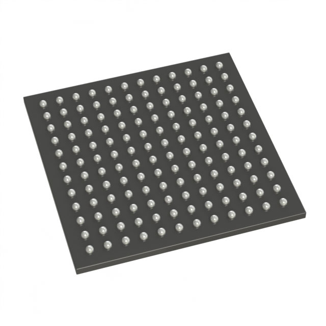
Overview of M1A3P1000-2FGG144 – ProASIC3 FPGA, 97 I/Os, 24,576 logic elements, 144-LBGA
The M1A3P1000-2FGG144 is a ProASIC3 family field programmable gate array (FPGA) featuring 24,576 logic elements and 97 user I/Os in a 144-LBGA package. This reprogrammable, nonvolatile flash-based FPGA is designed for low-power, instant-on applications where performance, integration and security are important.
Targeted at consumer, portable and battery-backed markets, the device combines on-chip embedded memory and flexible I/O to simplify system design while supporting mixed-voltage interfaces and in-system programming.
Key Features
- Core & Logic — 24,576 logic elements (cells) and a reported 1,000,000 equivalent system gates provide dense logic capacity for complex designs.
- Embedded Memory — 147,456 total RAM bits of on-chip memory (approximately 0.147 Mbits) plus on-chip Flash ROM for user nonvolatile storage.
- I/O Flexibility — 97 user I/Os with support for mixed-voltage operation across I/O banks, suitable for interfacing to 1.5V, 1.8V, 2.5V and 3.3V domains as indicated in the series datasheet.
- Security & In-System Programming — Series-level support for in-system programming with on-chip AES decryption and FlashLock to protect programmed contents.
- Performance — Series-level system performance characteristics include up to 350 MHz operation and segmented, hierarchical routing and clock structures for efficient timing.
- Power & Voltage — Core supply range of 1.425 V to 1.575 V and low-power architecture suited to power-sensitive designs.
- Package & Mounting — Surface-mount 144-LBGA (supplier device package 144-FPBGA, 13×13) for compact board integration and two-layer PCB friendliness.
- Operating Range & Compliance — Commercial grade operation from 0 °C to 85 °C; RoHS compliant.
Typical Applications
- Portable Consumer Electronics — Instant-on, low-power FPGA functionality for user interfaces, peripheral control and feature-rich consumer devices.
- Battery-backed Systems — Flash-based nonvolatile programmability and low core voltage make the device suitable for battery-powered equipment requiring retained configuration.
- High-volume, Cost-sensitive Products — Small-footprint 144-LBGA package and two-layer PCB compatibility support compact, high-volume designs.
- Interface and Glue Logic — Flexible mixed-voltage I/Os and abundant logic elements for protocol bridging, I/O aggregation and custom peripheral interfaces.
Unique Advantages
- Nonvolatile, Reprogrammable Solution: Flash-based architecture retains programmed design when powered off and supports in-system updates.
- High Logic Density: 24,576 logic elements enable implementation of complex control, glue logic and moderate signal-processing tasks on a single chip.
- Flexible I/O and Mixed-Voltage Support: A large number of user I/Os and bank-selectable voltages simplify integration with diverse external peripherals.
- Security and IP Protection: On-chip AES decryption and FlashLock features (series-level) support secure configuration and IP protection strategies.
- Compact, Surface-Mount Package: 144-LBGA (144-FPBGA 13×13) provides a small PCB footprint for space-constrained designs.
- Commercial Temperature Grade: Rated for 0 °C to 85 °C operation to match a wide range of commercial applications.
Why Choose M1A3P1000-2FGG144?
The M1A3P1000-2FGG144 delivers a balanced combination of logic capacity, embedded memory and flexible I/O in a compact 144-LBGA package. Its flash-based, reprogrammable architecture with on-chip nonvolatile storage supports instant-on behavior and in-field updates, while series-level security features help protect design IP.
This device is well suited for designers building cost- and power-sensitive consumer, portable, or battery-backed products that require a single-chip FPGA solution with substantial logic density and mixed-voltage interfacing.
Request a quote or submit a product inquiry to evaluate M1A3P1000-2FGG144 for your next design and to obtain pricing and availability information.


Date Founded: 1989
Headquarters: Chandler, Arizona, USA
Employees: 22,000+
Revenue: $8.349 Billion
Certifications and Memberships: ISO9001:2015, IATF16949:2016, AS 9100D


