
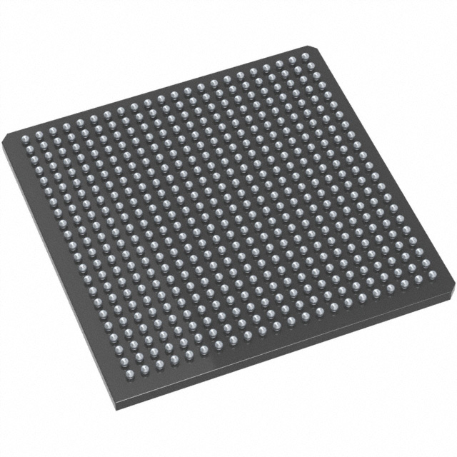
M1A3P1000-FGG484I
| Part Description |
ProASIC3 Field Programmable Gate Array (FPGA) IC 300 147456 484-BGA |
|---|---|
| Quantity | 1,743 Available (as of June 15, 2026) |
| Product Category | Field Programmable Gate Array (FPGA) |
|---|---|
| Manufacturer | Microchip Technology |
| Manufacturing Status | Active |
| Manufacturer Standard Lead Time | 18 Weeks |
| Datasheet |
Specifications & Environmental
| Device Package | 484-FPBGA (23x23) | Grade | Industrial | Operating Temperature | -40°C – 100°C | ||
|---|---|---|---|---|---|---|---|
| Package / Case | 484-BGA | Number of I/O | 300 | Voltage | 1.425 V - 1.575 V | ||
| Mounting Method | Surface Mount | RoHS Compliance | ROHS3 Compliant | REACH Compliance | REACH Unaffected | ||
| Moisture Sensitivity Level | 3 (168 Hours) | Number of LABs/CLBs | 24576 | Number of Logic Elements/Cells | 24576 | ||
| Number of Gates | 1000000 | ECCN | 3A991D | HTS Code | 8542.39.0001 | ||
| Qualification | N/A | Total RAM Bits | 147456 |
Overview of M1A3P1000-FGG484I – ProASIC3 Field Programmable Gate Array (FPGA) IC, 300 I/Os, 24,576 logic elements
The M1A3P1000-FGG484I is a ProASIC®3 flash-based FPGA offered by Microchip Technology. It combines nonvolatile, reprogrammable flash architecture with a high I/O count and a large logic fabric suitable for industrial embedded designs.
Designed for applications that require secure, low-power, instant-on operation and a compact high-pin-count package, this device targets portable, consumer and industrial systems that need dense logic, significant embedded RAM and flexible mixed-voltage I/O support.
Key Features
- Logic Fabric — 24,576 logic elements (versatile logic resources for glue logic, control, and custom processing functions).
- Embedded Memory — 147,456 bits of total on-chip RAM (approximately 0.147 Mbits) plus 1 kbit of FlashROM user nonvolatile memory for configuration or small user storage.
- I/O Density — 300 user I/O pins to support complex peripherals, bus interfaces and multi-channel sensor or actuator connections.
- Gate Capacity — Approximately 1,000,000 gates for moderate-to-high logic integration in a single device.
- Flash-Based, Reprogrammable Technology — Nonvolatile flash fabric enables instant-on operation and retains programmed design when powered off.
- Security and In-System Programming — On-chip 128-bit AES decryption for secure ISP via JTAG and FlashLock features to protect FPGA contents.
- High-Performance and Clocking — Series-level support for up to 350 MHz system performance and configurable clock conditioning circuitry including PLL options.
- Mixed-Voltage I/O — Support for 1.5V, 1.8V, 2.5V and 3.3V I/O standards with bank-selectable voltages and programmable drive/slew options.
- Power and Supply — Core supply range of 1.425 V to 1.575 V (centered on 1.5 V core operation) supporting low-power designs.
- Package and Mounting — 484-ball FPBGA in a 23 × 23 footprint (484-BGA); surface-mount package suitable for compact, high-density boards.
- Industrial Temperature Range — Rated for −40 °C to 100 °C operation for robust performance in industrial environments.
- Standards and Testability — JTAG (IEEE 1149.1) boundary-scan support for board-level test and ISP workflows.
Typical Applications
- Portable and Battery-Backed Devices — Instant-on flash operation and low core voltage make the device suitable for battery-powered consumer and portable systems.
- Industrial Control — High I/O count and industrial temperature rating support motor-control logic, sensor aggregation and I/O expansion in factory and process applications.
- Secure Embedded Systems — On-chip AES decryption and FlashLock support protect configuration data in security-sensitive applications and in-field updates.
- Interface Aggregation and Glue Logic — Large logic element count and abundant I/Os enable protocol bridging, bus interfacing and custom peripheral logic consolidation.
Unique Advantages
- Nonvolatile, Reprogrammable Flash: Retains configuration when powered off and enables in-system updates without external configuration memory.
- High I/O and Logic Density: 300 I/Os and 24,576 logic elements reduce the need for multiple devices when integrating complex logic and peripherals.
- Industrial Robustness: −40 °C to 100 °C operating range and surface-mount 484-FPBGA package accommodate demanding industrial environments and compact board layouts.
- Secure In-System Programming: 128-bit AES ISP via JTAG and FlashLock functionality protect IP and support secure deployment workflows.
- Flexible Mixed-Voltage I/Os: Bank-selectable I/O voltages across common logic families simplify board-level interfacing with varied peripheral voltages.
- Low-Voltage Core: 1.425–1.575 V supply range supports low-power system designs centered on 1.5 V core operation.
Why Choose M1A3P1000-FGG484I?
The M1A3P1000-FGG484I provides a balanced combination of nonvolatile flash-based FPGA architecture, substantial logic and RAM resources, and a high I/O count in a compact 484-BGA package. Its security features and in-system programming capability make it suitable for embedded designs that require protected updates and reliable field operation.
This device is well suited for engineers and procurement teams seeking a single-chip solution that consolidates glue logic, interfaces and custom processing while meeting industrial temperature requirements and mixed-voltage I/O needs.
Request a quote or submit an inquiry to check availability, pricing and lead times for the M1A3P1000-FGG484I. Our team can provide technical and purchasing support to help integrate this ProASIC3 device into your next design.


Date Founded: 1989
Headquarters: Chandler, Arizona, USA
Employees: 22,000+
Revenue: $8.349 Billion
Certifications and Memberships: ISO9001:2015, IATF16949:2016, AS 9100D


