
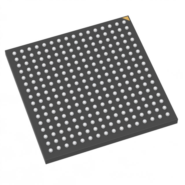
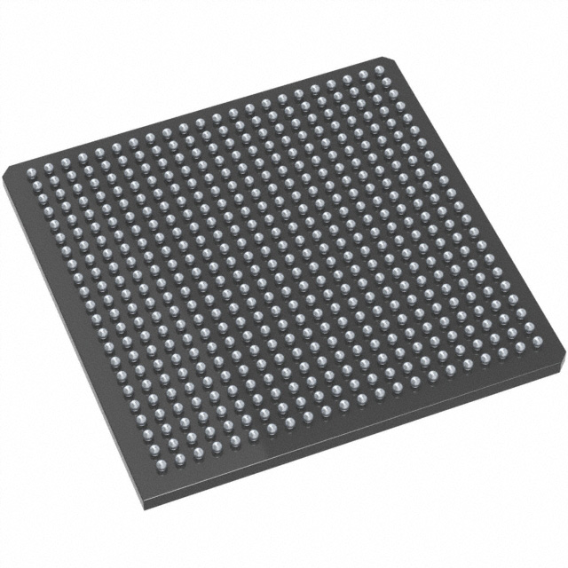
M1A3P1000-FGG256I
| Part Description |
ProASIC3 Field Programmable Gate Array (FPGA) IC 177 147456 256-LBGA |
|---|---|
| Quantity | 218 Available (as of June 18, 2026) |
| Product Category | Field Programmable Gate Array (FPGA) |
|---|---|
| Manufacturer | Microchip Technology |
| Manufacturing Status | Active |
| Manufacturer Standard Lead Time | 18 Weeks |
| Datasheet |
Specifications & Environmental
| Device Package | 256-FPBGA (17x17) | Grade | Industrial | Operating Temperature | -40°C – 100°C | ||
|---|---|---|---|---|---|---|---|
| Package / Case | 256-LBGA | Number of I/O | 177 | Voltage | 1.425 V - 1.575 V | ||
| Mounting Method | Surface Mount | RoHS Compliance | ROHS3 Compliant | REACH Compliance | REACH Unaffected | ||
| Moisture Sensitivity Level | 3 (168 Hours) | Number of LABs/CLBs | 24576 | Number of Logic Elements/Cells | 24576 | ||
| Number of Gates | 1000000 | ECCN | 3A991D | HTS Code | 8542.39.0001 | ||
| Qualification | N/A | Total RAM Bits | 147456 |
Overview of M1A3P1000-FGG256I – ProASIC3 Field Programmable Gate Array (FPGA), 177 I/O, 256-LBGA
The M1A3P1000-FGG256I is a reprogrammable, nonvolatile ProASIC3 Flash-based FPGA designed for applications that require secure, low-power, instant-on programmable logic in a compact package. Built for system-level integration, this device delivers 24,576 logic elements and a high I/O count for complex glue logic, control functions, and interface bridging in industrial and high-volume markets.
Its single-chip Flash architecture and support for mixed I/O voltages make it suitable for portable, battery-backed, and space-constrained designs where reduced BOM, rapid time-to-market, and retained configuration after power-down are important.
Key Features
- Logic Capacity 24,576 logic elements and approximately 1,000,000 system gates provide substantial programmable fabric for complex control and processing tasks.
- Embedded Memory Total on-chip RAM of 147,456 bits (approximately 0.147 Mbits) plus 1 kbit of FlashROM user nonvolatile memory for configuration and small data storage.
- I/O and Voltage Flexibility Up to 177 user I/Os with support for multiple I/O voltages; bank-selectable I/O enables mixed-voltage interfacing for modern system designs.
- Security and In-System Programming Supports in-system programming with on-chip AES-based decryption and Flash-based configuration retention for secure design updates and protected bitstreams.
- Low-Power Core Nominal core supply range of 1.425 V to 1.575 V supports low-power system architectures and 1.5 V-only systems.
- Package and Mounting 256-pin LBGA (supplier package: 256-FPBGA, 17×17) in a surface-mount form factor suited to compact PCB layouts.
- Industrial Temperature Grade Rated for operation from −40 °C to 100 °C for deployment in a wide range of industrial environments.
- RoHS Compliant Manufactured to meet RoHS requirements for environmental compliance.
Typical Applications
- Portable and Battery-Powered Devices Instant-on Flash configuration and low core voltage make the device suitable for portable electronics and battery-backed systems that need retained designs and low standby power.
- Consumer and High-Volume Products Compact 256-LBGA package and high logic density enable integration of glue logic, protocol conversion, and control functions in space- and cost-sensitive consumer products.
- Industrial Control and Automation Industrial temperature rating and extensive I/O count support robust control, monitoring, and interface tasks in factory and process automation applications.
- Secure In-System Updates On-chip AES-based ISP allows secure field updates and protected configuration management for devices requiring controlled firmware or hardware revisions.
Unique Advantages
- High-Density Programmable Fabric: 24,576 logic elements and ~1,000,000 gates provide ample resources to consolidate discrete logic and small processors into a single programmable device.
- Compact, High-I/O Package: 177 I/Os in a 256-LBGA (256-FPBGA 17×17) package reduces board area and simplifies high-density interconnect requirements.
- Nonvolatile, Instant-On Operation: Flash-based configuration retains design when powered off and eliminates the need for external configuration memory.
- Secure Field Programmability: On-chip AES decryption for in-system programming provides a mechanism for secure updates and protected bitstreams.
- Industrial Reliability: −40 °C to 100 °C operating range and surface-mount 256-LBGA packaging support deployment in demanding industrial environments.
- Low-Voltage Core: Narrow core supply range (1.425 V to 1.575 V) enables integration into low-power system architectures.
Why Choose M1A3P1000-FGG256I?
The M1A3P1000-FGG256I positions itself as a versatile, secure, and compact Flash FPGA suitable for applications that demand retained configuration, strong I/O density, and industrial temperature capability. With substantial logic and embedded RAM, it helps consolidate system functions, reduce BOM, and shorten development cycles for designs targeting portable, consumer, and industrial markets.
Its combination of nonvolatile Flash technology, AES-based in-system programming, and a high pin count in a small LBGA footprint delivers long-term value through simplified board design, secure update paths, and deployment flexibility across a wide temperature range.
If you would like pricing, availability, or technical support for the M1A3P1000-FGG256I, request a quote or submit an inquiry and our team will respond with details tailored to your project needs.


Date Founded: 1989
Headquarters: Chandler, Arizona, USA
Employees: 22,000+
Revenue: $8.349 Billion
Certifications and Memberships: ISO9001:2015, IATF16949:2016, AS 9100D


