
M1A3P1000-FGG144
| Part Description |
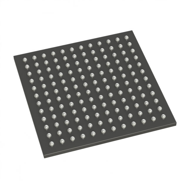
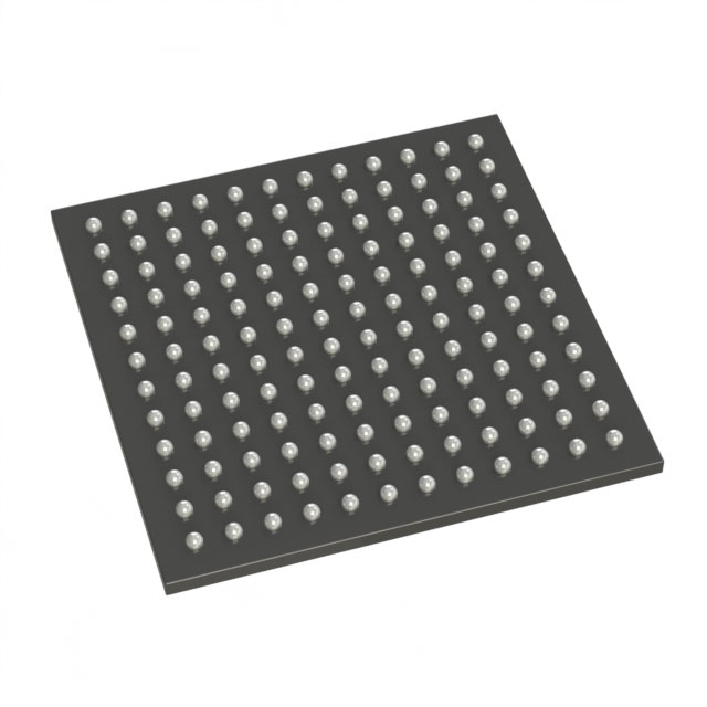
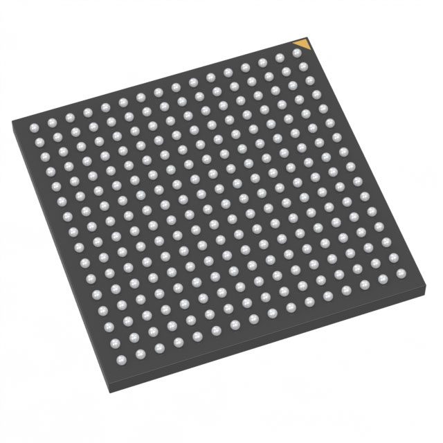
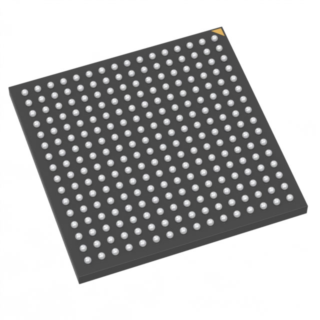
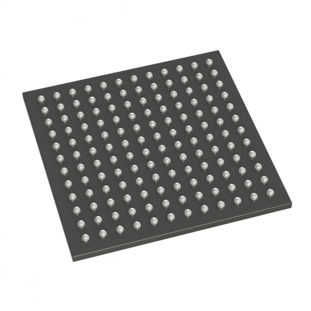
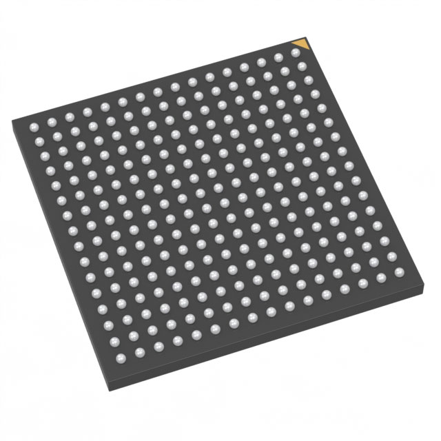
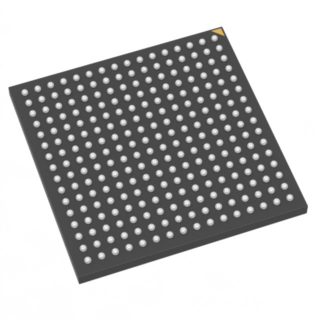
ProASIC3 Field Programmable Gate Array (FPGA) IC 97 147456 144-LBGA |
|---|---|
| Quantity | 1,280 Available (as of October 7, 2026) |
| Product Category | Field Programmable Gate Array (FPGA) |
|---|---|
| Manufacturer | Microchip Technology |
| Manufacturing Status | Active |
| Manufacturer Standard Lead Time | 18 Weeks |
| Datasheet |
Specifications & Environmental
| Device Package | 144-FPBGA (13x13) | Grade | Commercial | Operating Temperature | 0°C – 85°C | ||
|---|---|---|---|---|---|---|---|
| Package / Case | 144-LBGA | Number of I/O | 97 | Voltage | 1.425 V - 1.575 V | ||
| Mounting Method | Surface Mount | RoHS Compliance | ROHS3 Compliant | REACH Compliance | REACH Unaffected | ||
| Moisture Sensitivity Level | 3 (168 Hours) | Number of LABs/CLBs | 24576 | Number of Logic Elements/Cells | 24576 | ||
| Number of Gates | 1000000 | ECCN | 3A991D | HTS Code | 8542.39.0001 | ||
| Qualification | N/A | Total RAM Bits | 147456 |
Overview of M1A3P1000-FGG144 – ProASIC3 Field-Programmable Gate Array, 97 I/Os, 144-LBGA
The M1A3P1000-FGG144 is a Microchip ProASIC3 flash-based FPGA optimized for commercial designs that require reprogrammable, nonvolatile logic with mixed-voltage I/O support. This device combines high logic density, on-chip embedded RAM, and secure in-system programming features to address consumer, portable and other cost- and power-sensitive markets.
Architected as a single-chip, instant-on solution, the M1A3P1000-FGG144 is supplied in a compact 144-LBGA package and operates from a core supply range of 1.425 V to 1.575 V with a commercial temperature rating.
Key Features
- Logic Capacity — 24,576 logic elements (reported as Number Of Logic Elements Cells) and approximately 1,000,000 system gates provide substantial programmable resources for medium-to-high density designs.
- Embedded Memory — 147,456 total RAM bits of on-chip memory for FIFOs, buffers and small data stores.
- Flexible I/O — 97 user I/Os with support for mixed-voltage operation, enabling interfaces to 1.5V, 1.8V, 2.5V and 3.3V domains as appropriate for multi-voltage systems.
- Reprogrammable Flash-Based Architecture — Nonvolatile, instant-on flash technology for retained designs when powered off and in-system programmability.
- Security and In-System Programming — Series-level features include secure ISP mechanisms such as on-chip AES decryption and device content protection.
- Power and Voltage — Core supply specified from 1.425 V to 1.575 V, enabling low-power operation consistent with 1.5V-class FPGA cores.
- Package and Mounting — 144-LBGA surface-mount package (supplier package: 144-FPBGA, 13×13 mm) for compact board layouts.
- Commercial Temperature Grade — Operating range of 0°C to 85°C suitable for commercial applications.
- RoHS Compliant — Device complies with RoHS environmental requirements.
Typical Applications
- Portable Consumer Electronics — Low-voltage core and instant-on flash memory make this FPGA suitable for compact, battery-powered products requiring reprogrammable logic.
- Mixed-Voltage Interface Control — The device’s mixed-voltage I/O capability supports bridging and control between different supply domains in embedded systems.
- Secure In-System Programmability — On-chip AES-based ISP and FlashLock-style device protection are useful for products that require secure firmware updates and IP protection.
- Low-Power and Hot-Swap Capable Designs — Features described for the ProASIC3 family support low-power operation and hot-swap scenarios in cost-sensitive applications.
Unique Advantages
- High Logic Density: 24,576 logic elements and ~1,000,000 gates deliver substantial programmable capacity for complex functions without discrete glue logic.
- Nonvolatile, Reprogrammable Flash: Retains programmed designs when powered off and supports in-system updates, reducing the need for external configuration memory.
- Mixed-Voltage I/O Flexibility: Support for multiple I/O voltages enables seamless interfacing with a broad range of peripherals and ICs.
- Compact, Surface-Mount Packaging: The 144-LBGA (144-FPBGA 13×13) package supports high-density PCB layouts while maintaining robust I/O counts.
- Commercial Temperature and RoHS Compliance: Commercial-grade temperature range (0°C to 85°C) and RoHS compliance align with standard electronics manufacturing and environmental requirements.
- Secure ISP Capability: On-chip AES-based programming and content protection features help safeguard firmware and intellectual property.
Why Choose M1A3P1000-FGG144?
The M1A3P1000-FGG144 positions itself as a versatile, flash-based FPGA that balances logic capacity, embedded memory, and secure in-system programmability for commercial designs. Its combination of 24,576 logic elements, roughly 147 Kbits of on-chip RAM, and 97 mixed-voltage I/Os makes it well suited to designers targeting compact consumer and portable applications where retained configuration, low power, and interface flexibility matter.
Backed by the ProASIC3 family architecture, this device is appropriate for development teams seeking a reprogrammable, single-chip solution for cost- and power-conscious products that require secure updates and a compact board footprint.
Request a quote or submit a sales inquiry today to get pricing and availability for the M1A3P1000-FGG144.





















Date Founded: 1989
Headquarters: Chandler, Arizona, USA
Employees: 22,000+
Revenue: $8.349 Billion
Certifications and Memberships: ISO9001:2015, IATF16949:2016, AS 9100D




